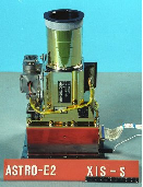
The X-ray Imaging Spectrometer (XIS, Koyama et al., 2007) celebrated its first light on 2006, August 11, about a month after the launch of Suzaku. The instrument has been operated successfully since then, producing many scientific results. The entire instrument has a weight of 48.7kg and consumes 67W at a bus voltage of 50V during normal operations. The XIS is composed of four units of Si-based X-ray charge coupled device (CCD) cameras (Fig. 7.1). In these X-ray sensors, incident X-ray photons are converted into a number of electron-hole pairs via photoelectric absorption and subsequent ionization by photoelectrons and their secondaries. The energy of the incident photon can be measured since it is proportional to the amount of charge produced.
Each XIS unit is located at the focal plane of one of four
independent, identical, and co-aligned X-Ray Telescope modules
(XRT, Serlemitsos et al., 2007), which are called XRT-I0, XRT-I1,
XRT-I2, and XRT-I3. The XIS is operated in photon-counting mode, in
which each X-ray event is discriminated from the others and its
position, energy, and arrival time are reconstructed. This gives the
XIS imaging-spectroscopic capabilities in the 0.2-12.0keV energy
band over an
![]() region.
region.
The XIS is similar to its predecessor, the Solid-state Imaging Spectrometer (SIS) onboard the ASCA satellite, in its working principle. Many improvements were made based on successful use of the SIS over eight years. It is also similar to its brothers: Chandra ACIS (Garmire et al., 2003), XMM-Newton EPIC (Turner et al., 2001; Strüder et al., 2001), and Swift XRT (Burrows et al., 2004).
X-ray CCD instruments, including the XIS, are characterized by their flexibility in operation and possible rapid performance changes on orbit. In particular, micro-meteorite hits can leave unrecoverable damage to a part of the instrument. The entire imaging area of the XIS2 was lost in 2005 November and a part of the XIS0 in 2009 June.
The XIS was developed and has been maintained jointly by Japan and the United States, with participating organizations including the MIT, ISAS, Kyoto University, Osaka University, Rikkyo University, Ehime University, Miyazaki University, Kogakuin University, Nagoya University, Aoyama Gakuin University, and major participating contractors including the Mitsubishi Heavy Industries (MHI), the NEC-Toshiba Space Systems, and the System Engineering Consultation (SEC) Co. Ltd.
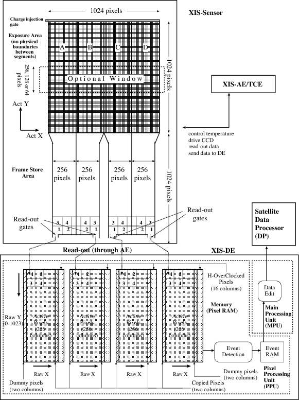
Each CCD camera has a single CCD chip, which consists of the imaging area and the frame store area. The imaging area is exposed to the sky for observations, while the frame store area is shielded. Each chip is composed of four segments called segment A, B, C, and D. Each segment has its own readout node (Fig. 7.3).
The imaging area has a pixel size of 1024![]() 1024 pixels. The
pixel scale is 24
1024 pixels. The
pixel scale is 24![]() m pixel
m pixel![]() and the physical size is 25mm
squared. The plate scale is 1.04
and the physical size is 25mm
squared. The plate scale is 1.04
![]() pixel
pixel![]() and the
total sky coverage is 18
and the
total sky coverage is 18![]() squared.
squared.
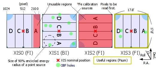
The XIS1 is a back-side illuminated (BI) chip. The other three sensors (XIS0, 2, and 3) are front-side illuminated (FI) chips. The BI and FI chips are superior to each other in the soft and hard band responses, respectively.
X-ray CCDs are also sensitive to optical and UV photons. To suppress such signals, an optical blocking filter (OBF) is installed on the surface of the CCDs. The OBF is made of polyimide with a thickness of 1000Å, which is coated with a total of 1200Å of Al (400Å on one side and 800Å on the other).
For in-flight calibration, three ![]() Fe calibration sources with a
half life of 2.73 years are installed in each XIS unit. The
Fe calibration sources with a
half life of 2.73 years are installed in each XIS unit. The ![]() Fe
sources emit strong Mn K
Fe
sources emit strong Mn K![]() and K
and K![]() lines at 5.9keV and
6.5keV, respectively. Two sources illuminate corners of the segments
A and D of the imaging area at the far side of the readout node. The
other one is installed in the door. It was used to illuminate the
entire chip before opening the door for the final check before launch
and the initial check after launch. Because the door was opened for
observations, the door calibration sources are not used any
longer. Scattered X-rays from the door calibration sources may appear
in the entire imaging area.
lines at 5.9keV and
6.5keV, respectively. Two sources illuminate corners of the segments
A and D of the imaging area at the far side of the readout node. The
other one is installed in the door. It was used to illuminate the
entire chip before opening the door for the final check before launch
and the initial check after launch. Because the door was opened for
observations, the door calibration sources are not used any
longer. Scattered X-rays from the door calibration sources may appear
in the entire imaging area.
To reduce the dark current, the sensors are kept at ![]() C
all the time. Thermo-electric coolers (TECs) using the Peltier effect
are used for cooling, which are controlled by the TEC Control
Electronics (TCE).
C
all the time. Thermo-electric coolers (TECs) using the Peltier effect
are used for cooling, which are controlled by the TEC Control
Electronics (TCE).
The analog electronics (AE) system drives the CCD by providing driving clocks for exposure and charge transfer, sampling the voltage, amplifying the data, and converting to the digital values. The XIS has two identical units of the AE and the TCE (see 7.1.2.2, Cooling system control), which are stored in the same housing for each unit. One unit (AE/TCE01) is used for XIS0 and XIS1, while the other (AE/TCE23) is used for XIS2 and XIS3.
The digital electronics (DE) system processes the digitized data. The DE has two pixel processing units (PPU01 and PPU23) and a main processing unit (MPU). The digital data from the AE are stored in the Pixel RAM of the PPUs; PPU01 for data taken with AE/TEC01 and PPU23 for AE/TEC23. The PPUs access the raw CCD data in the Pixel RAM, carry out event detection, and send event data to the MPU. The MPU edits the telemetry packets and sends them to the satellite's main digital processor.
Pixel data collected in each segment are read out from the corresponding readout node and sent to the Pixel RAM. In the Pixel RAM, pixels are given RAW X and RAW Y coordinates for each segment in the order of the readout, such that RAW X values are from 0 to 255 and RAW Y values are from 0 to 1023. These pixels in the Pixel RAM are named active pixels. In the same segment, pixels closer to the read-out node are read out earlier and stored in the Pixel RAM earlier. Hence, the order of the pixel read-out is the same for segments A and C, and for segments B and D, but different between these two segment pairs, because of the different locations of the readout nodes. In Fig. 7.3, numbers 1, 2, 3 and 4 marked on each segment and the Pixel RAM indicate the order of the pixel read-out and the storage in the Pixel RAM. In addition to the active pixels, the Pixel RAM stores copied pixels, dummy pixels and H-over-clocked pixels (Fig. 7.3). At the borders between two segments, two columns of pixels are copied from each segment to the other. Thus these are named copied pixels. Two columns of empty dummy pixels are attached to the segments A and D. In addition, 16 columns of H-over-clocked pixels are attached to each segment.
Actual pixel locations on the chip are calculated from the RAW XY coordinates and the segment ID during ground processing. The coordinates describing the actual pixel location on the chip are named ACT X and ACT Y coordinates (Fig. 7.3). It is important to note that the RAW XY to ACT XY conversion depends on the on-board data processing mode.
The detector performance changes both continuously and discontinuously over time. This is especially the case for CCD instruments. Users need to take the latest information into account in order to make the best use of the instrument. Some major changes and their causes are:
Table 7.1 shows major events since the start of the mission in chronological order. The XIS log at http://www.astro.isas.jaxa.jp/suzaku/log/xis/ gives a complete list of events relevant for data reduction.
The XIS has numerous instrumental settings, which are fine-tuned to serve a wide range of observational purposes. A few of them are left as user options. Different options can be used for different sensors.
In many cases, the default settings are adequate. If this is not the case, the appropriate choice of clocking mode options is generally enough and there is little need to change the other options. The choice between the XIS and HXD nominal positions is no longer available: all observations are made at the XIS nominal position (the center of the XIS field of view) unless otherwise requested.
Users need to consider an appropriate choice of clocking mode options
when they are planning observations of bright (![]() 10mCrab in
0.5-10keV) sources or those requiring a higher temporal resolution
than 8s.
10mCrab in
0.5-10keV) sources or those requiring a higher temporal resolution
than 8s.
Use of non-default options should be stated clearly in the technical justification of the proposal document. The choice of clocking mode needs to be specified in the cover page. These choices can be tentative. For successful proposals, an inquiry is sent to the PI about three weeks prior to the observation. The choice of user options can be revised at this time.
The behavior of very bright sources is often unpredictable. The XIS operation team waits until the last minute before finalizing the options, if necessary. The deadline is 10:00 JST (1:00 in UT) every weekday and Saturday, at which the operation team starts generating the command sequence. Users need to submit the final choice of options by this deadline 1-3 days before the start of their observation. Prior consultation with the XIS operation team is necessary for their availability and the exact deadline.
The appropriate choice of options is the responsibility of the
observer. A summary is provided by the XIS quick reference
at:
http://www.astro.isas.jaxa.jp/![]() tsujimot/pg_xis.pdf
tsujimot/pg_xis.pdf
The
XIS operation team can be consulted
at:
xisope@astro.iasa.jaxa.jp
The team will make the best
use of the operational flexibility to maximize the scientific output
of the observations.
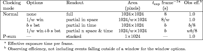
The clocking mode specifies how the CCD pixels are read out. Each
clocking mode has its own ![]() -code, a pattern of voltage clocking
for exposure and charge transfer. It enables full read, partial read,
or stacked read (Table 7.2). With a partial or
stacked read, a higher pile-up limit and timing resolution can be
achieved at a sacrifice of observing efficiency and imaging
information.
-code, a pattern of voltage clocking
for exposure and charge transfer. It enables full read, partial read,
or stacked read (Table 7.2). With a partial or
stacked read, a higher pile-up limit and timing resolution can be
achieved at a sacrifice of observing efficiency and imaging
information.
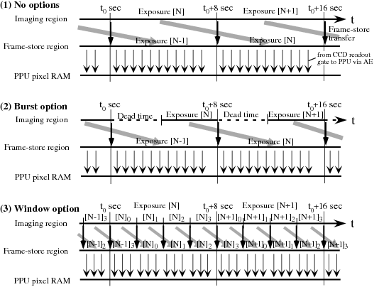
There are two major types of clocking mode: the Normal mode and the P-sum mode. The Normal mode is for timed-exposure readout. It can be combined with a window option (partial readout in space), burst option (partial readout in time), or both (partial readout in both space and time). Fig. 7.4 shows the time sequence of exposure, frame-store transfer, readout, and storage to the Pixel RAM (in the PPU) for the Normal clocking mode. The P-sum mode is for stacked readout. The P-sum clocking mode is in principle available for all FI sensors. However, because it is severly affected by leaked charge in areas damaged by micrometerorite hits, the P-sum clocking support was terminated for the XIS2 and XIS0. Therefore, it is currently available only for the XIS3. Observers using the P-sum clocking mode for the XIS3 need to use a Normal clocking mode for the other sensors.
|
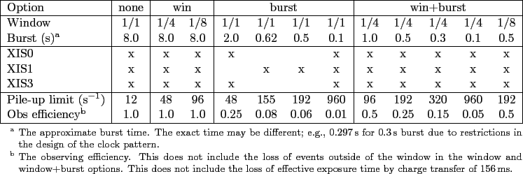
The available window and burst options are summarized in Table 7.3.
The pulse height from 128 rows are stacked into a single row along the
Y direction. Charge is transferred continuously, thus the spatial
information along the Y direction is lost and replaced with the
arrival time information. The arrival time is ticked at a 7.8ms
resolution. This is smeared by the point spread function with a HPD of
2![]() , which is equivalent to 0.9s.
, which is equivalent to 0.9s.
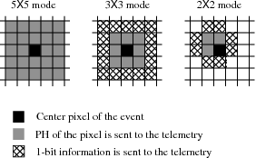
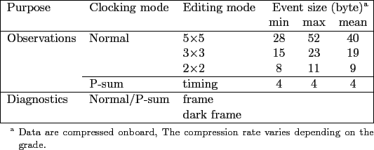
The editing mode specifies the telemetry format of the events. The XIS has several editing modes (Table 7.4). Four of them are for observational purposes, the remaining ones are for diagnostic purposes.
For Normal clocking modes three editing modes (5![]() 5, 3
5, 3![]() 3,
and 2
3,
and 2![]() 2) are available. The 2
2) are available. The 2![]() 2 mode is used only for
the FI sensors. For P-sum clocking mode, the editing mode is fixed to
the timing mode. Each editing mode has a different telemetry format,
which includes the x and y position and the pulse height (PH) of the
event (Fig. 7.5). Different editing modes have
different sizes per event (Table 7.4).If the
dark-subtracted PH value is above the split threshold in the
neighboring pixels, they are considered to be a part of the charges
generated by the event and thus are summed in the event
reconstruction. Different thresholds are applied for the immediately
neighboring pixels (inner split threshold) and those around them
(outer split threshold).
2 mode is used only for
the FI sensors. For P-sum clocking mode, the editing mode is fixed to
the timing mode. Each editing mode has a different telemetry format,
which includes the x and y position and the pulse height (PH) of the
event (Fig. 7.5). Different editing modes have
different sizes per event (Table 7.4).If the
dark-subtracted PH value is above the split threshold in the
neighboring pixels, they are considered to be a part of the charges
generated by the event and thus are summed in the event
reconstruction. Different thresholds are applied for the immediately
neighboring pixels (inner split threshold) and those around them
(outer split threshold).
|
Although the amount of information for event reconstruction is
different among the 5![]() 5, 3
5, 3![]() 3, and 2
3, and 2![]() 2 modes, no
significant difference has been found so far between the former two
modes. Only a small difference is seen for the 2
2 modes, no
significant difference has been found so far between the former two
modes. Only a small difference is seen for the 2![]() 2 mode for its
lack of ability to perform trail correction (§ 7.3.2.4). The
2
2 mode for its
lack of ability to perform trail correction (§ 7.3.2.4). The
2![]() 2 mode and the timing mode are not available for the XIS1
because the trailing correction does not work properly for the former
mode and the amount of flickering pixel is larger than for the other
sensors for the latter mode.
2 mode and the timing mode are not available for the XIS1
because the trailing correction does not work properly for the former
mode and the amount of flickering pixel is larger than for the other
sensors for the latter mode.
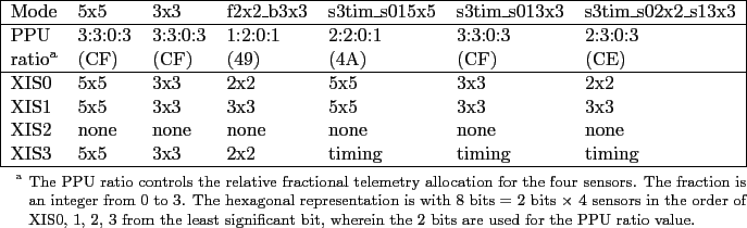
Technically speaking, arbitrary combinations of editing modes for the four sensors are possible. However, for reasons of operational reliability, combinations are restricted to those listed in Table 7.5.
The diagnositic modes are only for diagnostic purposes and not available to general users. The XIS is operated in these modes outside of observing times.
The PPU ratio controls the relative fractional telemetry allocation
for the four sensors. The ratio is fixed to be the optimum value
assuming the use of the Normal clocking mode with the same options for
all the sensors (5x5, 3x3, or f2x2_b3x3 combination) or the use of
the P-sum clocking mode for XIS3 and the Normal clocking mode with the
1/4win ![]() 0.5s burst option for XIS0 and 1 (s3tim_s015x5,
s3tim_s013x3, or s3tim_s02x2_s13x3 combination).
0.5s burst option for XIS0 and 1 (s3tim_s015x5,
s3tim_s013x3, or s3tim_s02x2_s13x3 combination).
The lower event threshold defines the pulse height above which an event is recognized. It practically controls the lowest bandpass of the detector. The default event threshold is shown in Table 7.6. For XIS calibration observations, the FI event threshold is set to 50.
A part of the image can be masked with an area discrminator. Either the inside or the outside of a single rectangular region can be applied as a mask separately for each sensor. This is useful to supress telemetry of unwanted bright sources within the field of view of the target source. Currently, an area discrimination mask is applied permanently to the XIS0 to suppress leaked charge from the area damaged by a micrometeorite hit.
Photon pile-up is caused when multiple photons arrive at a detection
cell within the frame time. If two photons with energies of ![]() and
and ![]() arrive, they are wrongly recognized as a single photon
with an energy of
arrive, they are wrongly recognized as a single photon
with an energy of ![]() . This causes underestimation of the
count rate, spectral hardening, PSF distortion, grade migration, and
various other effects. Photon pile-up is a concern in observing
point-like sources brighter than
. This causes underestimation of the
count rate, spectral hardening, PSF distortion, grade migration, and
various other effects. Photon pile-up is a concern in observing
point-like sources brighter than ![]() 10mCrab. The degree of
pile-up is measured by the pile-up fraction. Assume the mean count
rate of photons landing in a pixel is
10mCrab. The degree of
pile-up is measured by the pile-up fraction. Assume the mean count
rate of photons landing in a pixel is
![]() s
s![]() pixel
pixel![]() . Then, the mean number of counts
(
. Then, the mean number of counts
(![]() ) in a detection cell (
) in a detection cell (
![]() ) within the
frame time (
) within the
frame time (
![]() ) is
) is
The number (![]() ) fluctuates around
) fluctuates around ![]() following Poisson
statistics. The probability to have
following Poisson
statistics. The probability to have ![]() photons in a detection cell
within the frame time is
photons in a detection cell
within the frame time is
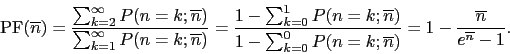
The pile-up fraction (PF) is defined as the fraction of pile-up events
among all incoming events as
Obviously,
![]() as
as
![]() and
and
![]() as
as
![]() .
.
![]() is a function of the position in the PSF
is a function of the position in the PSF
![]() as
as
The pile-up limit is defined as the total count rate
(
![]() s
s![]() ) at which the PF(
) at which the PF(![]() ) at
the center of the PSF exceeds 3%. In the XIS, this happens at roughly
12s
) at
the center of the PSF exceeds 3%. In the XIS, this happens at roughly
12s![]() , or 10mCrab. The limit should be regarded as an
approximate value as the exact value depends on the spectral shape of
the observed target. The tolerance also depends on scientific
goals. For example, if the detection of a weak hard tail is the goal,
the pile-up effect should be minimized. If the detection of a line is
the goal, some degree of pile-up can be tolerated.
, or 10mCrab. The limit should be regarded as an
approximate value as the exact value depends on the spectral shape of
the observed target. The tolerance also depends on scientific
goals. For example, if the detection of a weak hard tail is the goal,
the pile-up effect should be minimized. If the detection of a line is
the goal, some degree of pile-up can be tolerated.
|
| Radius | Pile-up fraction | ||
| (pixel) | |||
| 3% | 20% | 50% | |
| 13.4 | 30.0 | 45.9 | |
| 5 |
17.6 | 43.3 | 67.7 |
| 10 |
25.6 | 64.3 | 101 |
| 15 |
33.8 | 85.4 | 134 |
| 20 |
42.6 | 108 | 171 |
| 25 |
55.8 | 142 | 224 |
| 30 |
70.6 | 180 | 285 |
| 35 |
88.2 | 226 | 356 |
| 40 |
100 | 256 | 404 |
| 45 |
119 | 304 | 480 |
| 50 |
141 | 362 | 571 |
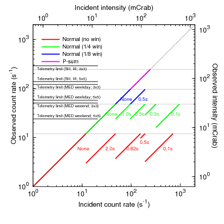
There are two major strategies to mitigate the effects of
pile-up. They can be used together. One is to raise the pile-up limit
by using an option in the Normal clocking mode. The pile-up
limit for various options is summarized in
Table 7.3 and shown in
Fig. 7.6. The other is to only use events from the
outskirts of the PSF, where the incoming rate per pixel is
substantially smaller than in the center. This is called the
annulus extraction method and is discussed in detail in
Yamada et al. (2011). The tools are available
at
http://www-utheal.phys.s.u-tokyo.ac.jp/![]() yamada/soft/XISPileupDoc_20120221/XIS_PileupDoc_20120220.html.
yamada/soft/XISPileupDoc_20120221/XIS_PileupDoc_20120220.html.
Table 7.7
gives the total incoming rate, at which some representative pile-up
limit is hit at various radii in the PSF. In this approach, the
fraction of grade 1 events is known to be a good indicator to assess
the degree of pile-up. Note that the attitude fluctuation of
the satellite does not mitigate the photon pile-up as its typical
time scale is much longer than the frame time of 8s.
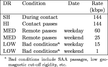
The XIS has a quota for the size of telemetry per unit time. The quota
depends on the data rates (DR; SH![]() super high, HI
super high, HI![]() high,
MED
high,
MED![]() medium, and LOW
medium, and LOW![]() low) and whether the observation is conducted
on weekends or weekdays (Table 7.8). The
satellite is also operated with a weekend allocation for a few days at
the end and the beginning of the year. The operations team is
responsible for deciding on the data rates depending on the observing
conditions. The schedule is made to avoid bright sources to be
observed on weekends, during which the telemetry allocation is
small. Possible excess use of the quota is determined every 8s during
observations. Beyond the limit, a part of the telemetry is
lost. Events in the segments B and C are prioritized over those in the
segments A and D. Telemetry saturation occurs only when observing
bright sources. Fortunately, in the XIS, the telemetry saturation is
always avoided when users select an appropriate clocking mode to avoid
pile-up. In practice, the following users need to consider the possibility
of telemetry saturation seriously:
low) and whether the observation is conducted
on weekends or weekdays (Table 7.8). The
satellite is also operated with a weekend allocation for a few days at
the end and the beginning of the year. The operations team is
responsible for deciding on the data rates depending on the observing
conditions. The schedule is made to avoid bright sources to be
observed on weekends, during which the telemetry allocation is
small. Possible excess use of the quota is determined every 8s during
observations. Beyond the limit, a part of the telemetry is
lost. Events in the segments B and C are prioritized over those in the
segments A and D. Telemetry saturation occurs only when observing
bright sources. Fortunately, in the XIS, the telemetry saturation is
always avoided when users select an appropriate clocking mode to avoid
pile-up. In practice, the following users need to consider the possibility
of telemetry saturation seriously:
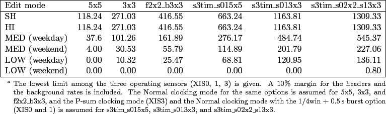
The telemetry saturation limit depends on the DR, choice of clocking
modes, editing modes, and the PPU ratio. The resultant telemetry
saturation limits are shown in
Table 7.9 for the six editing mode
combinations. A 10% margin for the headers and the background rates
of 10s![]() (FI) and 20s
(FI) and 20s![]() (BI) are included. The exact
limit depends on the choice of clocking mode options. Users can use
the XIS limit calculator at
(BI) are included. The exact
limit depends on the choice of clocking mode options. Users can use
the XIS limit calculator at
http://www.astro.isas.jaxa.jp/![]() tsujimot/limits_xis.ods.
tsujimot/limits_xis.ods.
The operations team is fully responsible for an appropriate choice of editing mode combinations among those in Table 7.5. The PPU ratio is optimized for a wide range of cases. Therefore, not much can be done by users in the observation planning stage to avoid telemetry saturation. In the data analysis step, however, users can remove time intervals afflicted by saturation by filtering the events using the distributed ``non-saturated'' good time interval files. The detailed procedure can be found in section 6.5.1 of the Suzaku Data Reduction Guide (ABC Guide).
Out-of-time events are events recorded during charge transfer. They
spread along the Y direction beyond the PSF with low surface
brightness. For accurate photometry, users might need to take
out-of-time events into account. It is expected that they have the
same spectrum as the on-source events. The effect is present for the
Normal clocking mode with any option, but is different for
observations with and without burst option. For the Normal clocking
mode without burst option, the out-of-time events spread uniformly
along the Y direction at a surface brightness of
156ms/(8-0.156)s![]() 2.0% integrated over 1024pixels. For the
Normal clocking mode with a
2.0% integrated over 1024pixels. For the
Normal clocking mode with a ![]() s burst option, the out-of-time
events spread uniformly in the upper and lower half of the image with
different strengths (Fig. 7.7). This happens
because the clocking of the
s burst option, the out-of-time
events spread uniformly in the upper and lower half of the image with
different strengths (Fig. 7.7). This happens
because the clocking of the ![]() s burst options consists of several
steps: (1) exposure for
s burst options consists of several
steps: (1) exposure for ![]() (8-
(8-![]() )s, (2) charge transfer only in
the imaging area for flushing, (3) exposure for
)s, (2) charge transfer only in
the imaging area for flushing, (3) exposure for ![]() s, (4) charge
transfer both in the imaging and storing areas for recording. In (2),
the flushing readout is performed with charge injection and takes
156ms. In (4), the recording readout is performed without charge
injection and takes 25ms. The different strengths in the upper and
lower half of the image are caused by this. The fraction of
out-of-time events is
s, (4) charge
transfer both in the imaging and storing areas for recording. In (2),
the flushing readout is performed with charge injection and takes
156ms. In (4), the recording readout is performed without charge
injection and takes 25ms. The different strengths in the upper and
lower half of the image are caused by this. The fraction of
out-of-time events is ![]() 25ms/
25ms/![]() /2s in the upper part and
/2s in the upper part and
![]() 156ms/
156ms/![]() /2s in the lower part. The fraction can be
significant for short burst options, i.e., for the 0.1s burst
option, the out-of-time events amount to 12.5% in the upper half and
78% in the lower half.
/2s in the lower part. The fraction can be
significant for short burst options, i.e., for the 0.1s burst
option, the out-of-time events amount to 12.5% in the upper half and
78% in the lower half.
|
The contribution of out-of-time events can be estimated in the area far from the center of the image. This is difficult for observations taken with a window mode. In such cases, at least one of the sensors can be operated without a window option so that it can be used for estimating the out-of-time events also for other sensors.
In principle, charge traps can be filled not only by artificially injected charges, but also by charges created by X-ray events. This effect is apparent in observations of some very bright sources (Todoroki et al., 2012). This effect is not included in the calibration. Users may encounter a better energy resolution than the distributed RMF files indicate.
X-ray CCD devices are subject to degradation in orbit. One of the outcomes is an increase of charge traps under the constant radiation of cosmic rays in the space environment. This results in an increase of the charge transfer inefficiency (CTI), which leads to a degradation of the energy resolution.
|
The XIS has a function to precisely monitor and mitigate this
effect. For monitoring each sensor has ![]() Fe calibration sources
at two corners on the far-side of the readout. For mitigation
spaced-row charge injection (SCI) is implemented. Electrons are
injected artificially from one side of the chip and are read out along
with charges produced by X-ray events. The artificial charges are
injected periodically in space (every 54 rows;
Fig. 7.8). They fill up charge traps and thereby
alleviate the increase in CTI for charges by X-ray events
(Ozawa et al., 2009; Bautz et al., 2004; Uchiyama et al., 2009; Nakajima et al., 2008). SCI is not
available for the P-sum clocking mode for its continuous clocking
nature.
Fe calibration sources
at two corners on the far-side of the readout. For mitigation
spaced-row charge injection (SCI) is implemented. Electrons are
injected artificially from one side of the chip and are read out along
with charges produced by X-ray events. The artificial charges are
injected periodically in space (every 54 rows;
Fig. 7.8). They fill up charge traps and thereby
alleviate the increase in CTI for charges by X-ray events
(Ozawa et al., 2009; Bautz et al., 2004; Uchiyama et al., 2009; Nakajima et al., 2008). SCI is not
available for the P-sum clocking mode for its continuous clocking
nature.
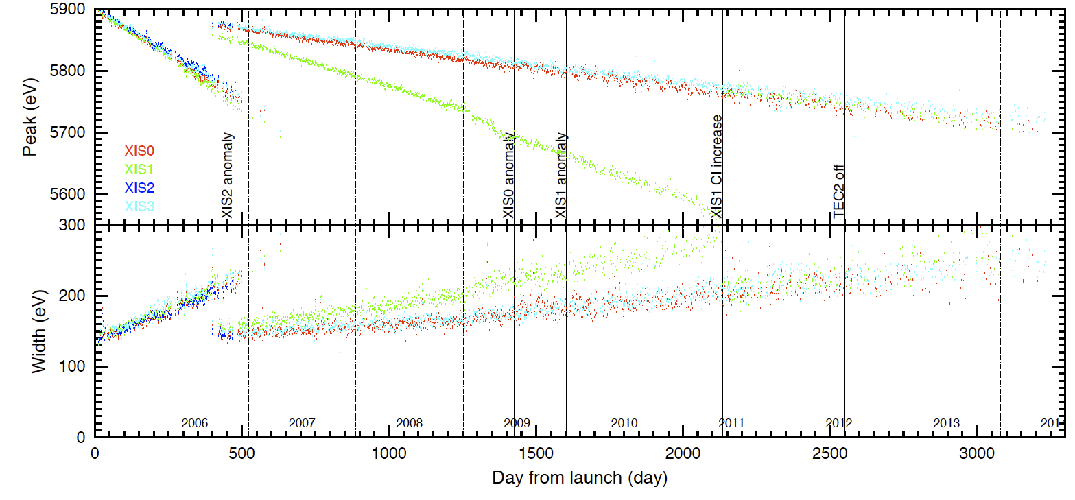
Fig. 7.9 shows the long-term trend of the measured peak
energy and width of the Mn I K![]() line (5.9keV) from the
calibration sources. The peak energy decreases and the width increases
gradually. Both quantities are restored by applying SCI.
line (5.9keV) from the
calibration sources. The peak energy decreases and the width increases
gradually. Both quantities are restored by applying SCI.
|
The SCI technique was put into routine operation in the middle of 2006 and has brought a drastic improvement. At the start of SCI operations, it was decided to inject the amount of charges equal to the amount produced by a 6keV X-ray photon (``6 keV equivalent'') for the FI devices and a smaller amount (``2 keV equivalent'') for the BI device. The smaller amount for XIS1 was chosen to minimize the expected SCI-related increase in noise in the soft spectral band, at which the BI device has an advantage over the FI device.
The choice between SCI on and SCI off was a user option for nearly one year after the start of SCI operations. This was because SCI observations suffer from a larger dead area and a larger fraction of out-of-time events in addition to providing an improved spectroscopic performance. The user option was terminated and all observations have been made exclusively with SCI on since AO4, as the number of users choosing SCI off had decreased substantially.
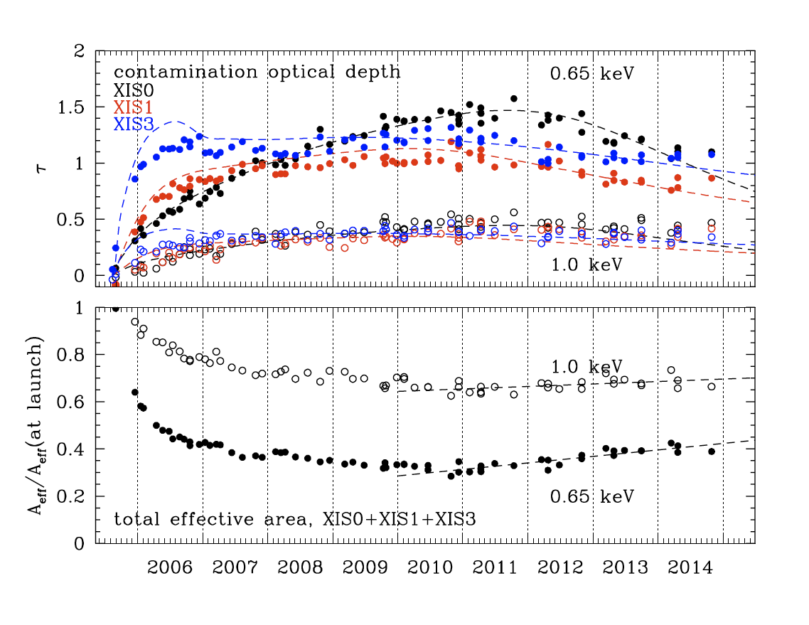
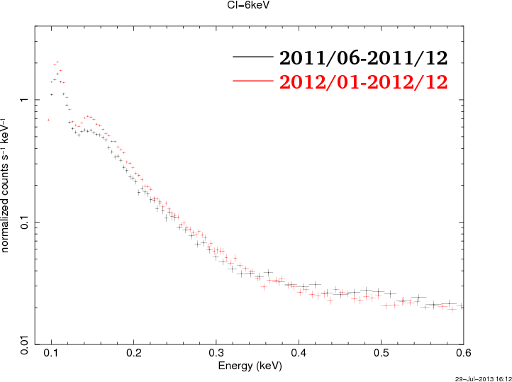
The accumulation of contaminating material on the surface of the CCDs made the soft-band advantage of the BI sensor less prominent (§ 7.3.3). The CTI for the BI device has increased at a faster rate due to the smaller amount of injection charges. As a consequence, the astrophysically important lines of Fe XXV (6.7keV) and Fe XXVI (7.0keV) became hardly resolved in 2010. The injection charge amount was changed from 2keV to 6keV equivalent for the BI sensor according to the schedule of Table 7.1. Detailed information can be found in the Suzaku memo 2010-07 available at http://www.astro.isas.ac.jp/suzaku/doc/suzakumemo/suzakumemo-2010-07v4.pdf.
Users need to be aware of some drawbacks associated with the SCI operations:
The calibration of the spectroscopic performance of the XIS mainly consists of calibrating the energy gain and resolution. Regarding the energy gain, corrections for charge trails and for the CTI are performed.
For the energy resolution, the time-dependence is modeled as
| (7.5) |
For the normal clocking modes, data taken with the 3![]() 3 and
5
3 and
5![]() 5 editing modes are merged, since it is known that their
differences are negligible.
5 editing modes are merged, since it is known that their
differences are negligible.
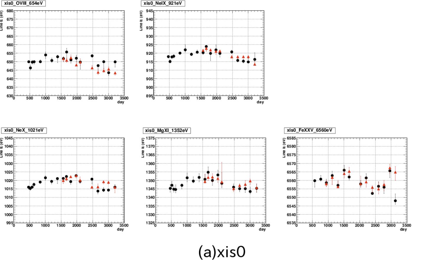
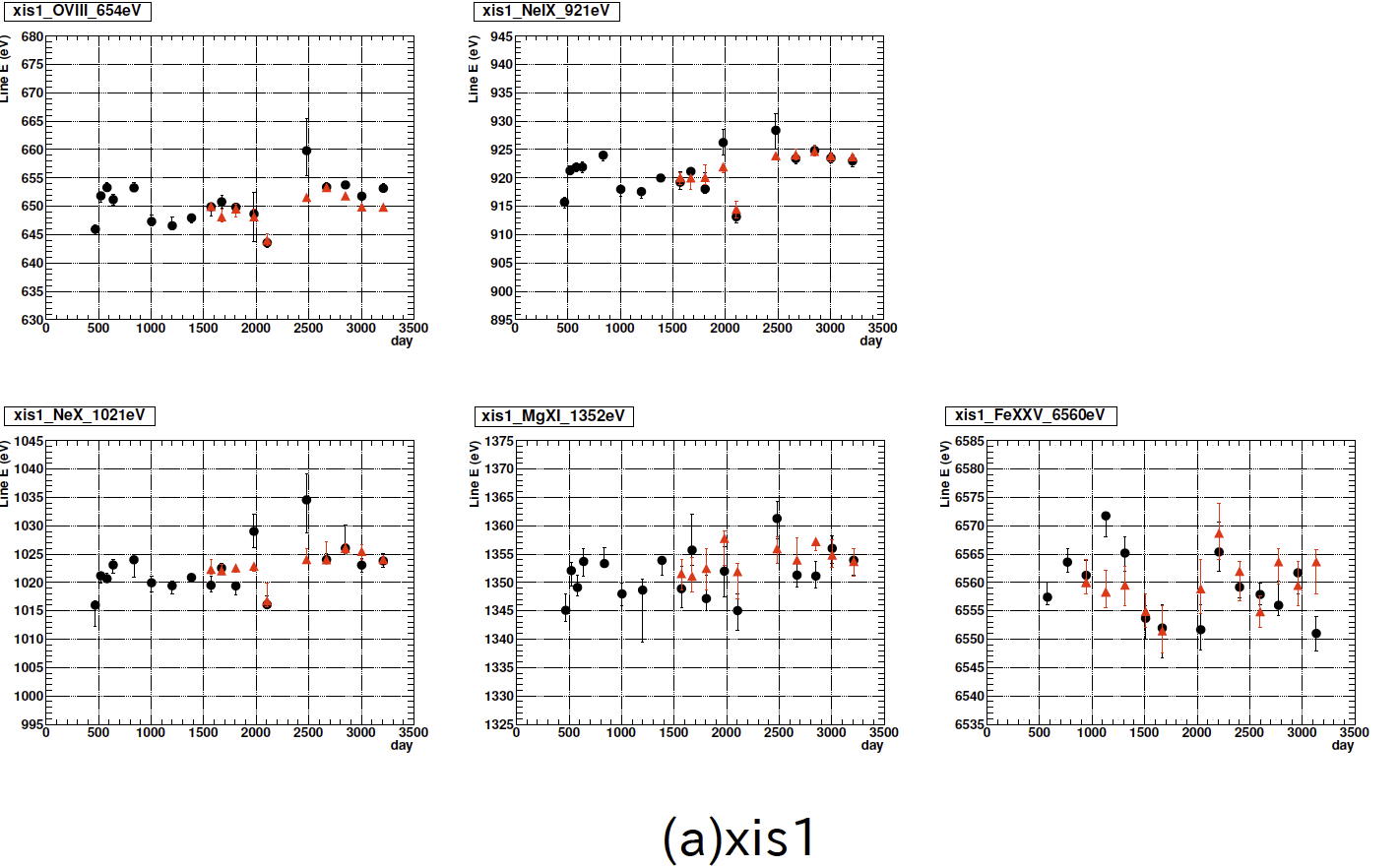
The Normal mode without options is the best calibrated mode of the
XIS. The CTI is measured using observations of the Perseus Cluster
(all segments, hard band), 1E0102![]() 72 (segments B and C, soft band),
and the
72 (segments B and C, soft band),
and the ![]() Fe calibration sources (segments A and D, hard
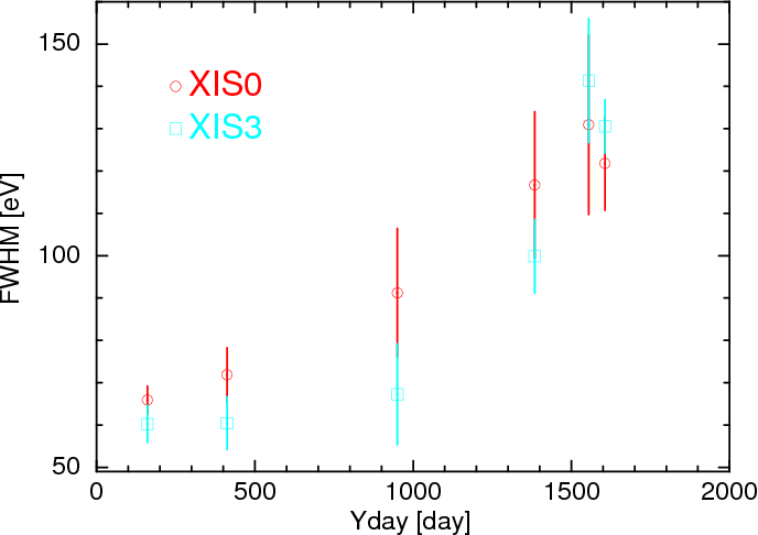
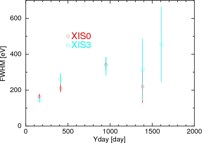
band). Fig. 7.10 and 7.11,
respectively, show the gain and energy resolution in the hard band
using the
Fe calibration sources (segments A and D, hard
band). Fig. 7.10 and 7.11,
respectively, show the gain and energy resolution in the hard band
using the ![]() Fe calibration sources, while
Fig. 7.12 and 7.13,
respectively, show the gain and energy resolution in the soft band
using the E0102
Fe calibration sources, while
Fig. 7.12 and 7.13,
respectively, show the gain and energy resolution in the soft band
using the E0102![]() 72 observations.
72 observations.
![\includegraphics[width=1.00\textwidth]{figures_xis/fig10_MnKaCenter}](img195.png)
|
![\includegraphics[width=1.00\textwidth]{figures_xis/fig11_MnKaWidth}](img196.png)
|
![\includegraphics[width=1.00\textwidth]{figures_xis/fig12_OLyaCenter}](img197.png)
|
![\includegraphics[width=1.00\textwidth]{figures_xis/fig13_OLyaWidth}](img198.png)
|
Since the ![]() Fe calibration sources are unavailable for
observations with window options, the Perseus Cluster is regularly
observed with the 1/4 window option for calibration purposes
(Table 7.10). The target is observed in Normal mode twice, without
option and with 1/4 window option, with consecutive exposures, in
order to construct a comparison data set at each epoch. No calibration
sources are observed with the 1/8 window option. The pulse height
correction for the Normal mode with window option is the same as that
for the Normal mode without options, except that they use different
numbers of fast and slow charge transfers. Fast and slow transfers are
used for reading out the effective imaging area and the non-imaging
area, respectively. They have different CTIs. For the window options,
the non-imaging area includes the frame store area as well as the
imaging area outside of the window. The CTI for each transfer is
calibrated using the calibration observations with the 1/4 window
option, which is also applied to the 1/8 window
option. Fig. 7.14, 7.15, and
7.16 show the resulting gain using several emission
lines, comparing the Normal mode without options and the Normal mode
with 1/4 window option. The two gain calibrations are consistent to
within
Fe calibration sources are unavailable for
observations with window options, the Perseus Cluster is regularly
observed with the 1/4 window option for calibration purposes
(Table 7.10). The target is observed in Normal mode twice, without
option and with 1/4 window option, with consecutive exposures, in
order to construct a comparison data set at each epoch. No calibration
sources are observed with the 1/8 window option. The pulse height
correction for the Normal mode with window option is the same as that
for the Normal mode without options, except that they use different
numbers of fast and slow charge transfers. Fast and slow transfers are
used for reading out the effective imaging area and the non-imaging
area, respectively. They have different CTIs. For the window options,
the non-imaging area includes the frame store area as well as the
imaging area outside of the window. The CTI for each transfer is
calibrated using the calibration observations with the 1/4 window
option, which is also applied to the 1/8 window
option. Fig. 7.14, 7.15, and
7.16 show the resulting gain using several emission
lines, comparing the Normal mode without options and the Normal mode
with 1/4 window option. The two gain calibrations are consistent to
within ![]() 5eV over the entire energy band for the whole mission
to date.
5eV over the entire energy band for the whole mission
to date.
|
|
|
For the calibration of the Normal mode with burst option advantage is
taken of the Crab calibration observations (which are primarily
performed for HXD calibration purposes). Since the Crab has a
featureless spectrum, the ![]() Fe calibration source spectra are
used in addition (Table 7.10). In the Normal mode with burst
option no correction is made in addition to those for the Normal mode
without options. The calibration observations are only used to confirm
that there is no change in the instrumental response for the burst
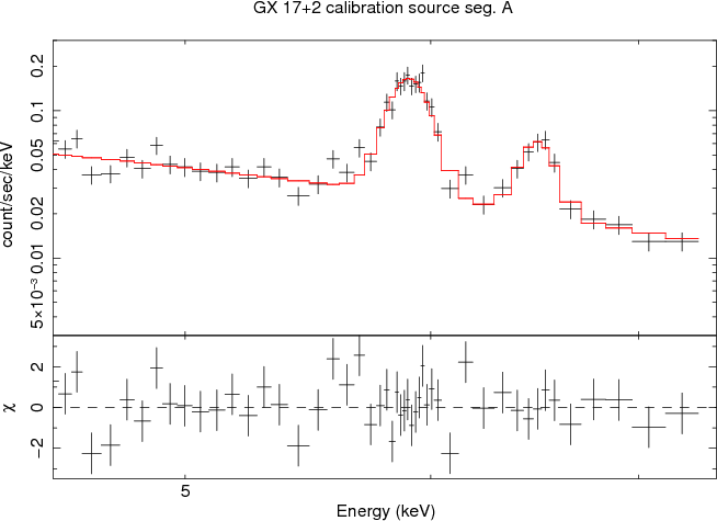
options. Fig. 7.17 shows a
Fe calibration source spectra are
used in addition (Table 7.10). In the Normal mode with burst
option no correction is made in addition to those for the Normal mode
without options. The calibration observations are only used to confirm
that there is no change in the instrumental response for the burst
options. Fig. 7.17 shows a ![]() Fe calibration source
spectrum taken with the 2.0s burst option during an observation of
GX 17
Fe calibration source
spectrum taken with the 2.0s burst option during an observation of
GX 17![]() 2. It has been modeled using the RMF for the Normal mode
(without options). There is no structure in the residuals. This is
indicating that the response is the same for the Normal mode without
options and the Normal mode with the 2.0s burst option.
2. It has been modeled using the RMF for the Normal mode
(without options). There is no structure in the residuals. This is
indicating that the response is the same for the Normal mode without
options and the Normal mode with the 2.0s burst option.
|
|
The data taken with the 2![]() 2 editing mode have insufficient
information to conduct trail correction around each event, unlike those
taken with the 3
2 editing mode have insufficient
information to conduct trail correction around each event, unlike those
taken with the 3![]() 3 or 5
3 or 5![]() 5 editing modes. It is therefore
inevitable for the 2
5 editing modes. It is therefore
inevitable for the 2![]() 2 editing mode to have different gain
compared to the other editing modes. In particular, the gain
difference between 3
2 editing mode to have different gain
compared to the other editing modes. In particular, the gain
difference between 3![]() 3/5
3/5![]() 5 and 2
5 and 2![]() 2 depends on the
ACTY position of the imaging area. Since the 2
2 depends on the
ACTY position of the imaging area. Since the 2![]() 2 editing mode
is only used for very bright point-like sources for the purpose of
reducing telemetry and since these observations are made at the XIS
nominal position, the 2
2 editing mode
is only used for very bright point-like sources for the purpose of
reducing telemetry and since these observations are made at the XIS
nominal position, the 2![]() 2 editing mode data are calibrated such
that the gain difference between 3
2 editing mode data are calibrated such
that the gain difference between 3![]() 3/5
3/5![]() 5 and 2
5 and 2![]() 2
modes is minimal at the image center. Fig. 7.19 shows
the difference of the 2
2
modes is minimal at the image center. Fig. 7.19 shows
the difference of the 2![]() 2 and 5
2 and 5![]() 5 editing mode gains in
the soft and hard energy bands at several different ACTY positions. At
the center (ACTY
5 editing mode gains in
the soft and hard energy bands at several different ACTY positions. At
the center (ACTY![]() 512), the difference is within
512), the difference is within ![]() 3eV. For
calibration purposes, 2
3eV. For
calibration purposes, 2![]() 2 editing mode data are artificially
generated on the ground using the 3
2 editing mode data are artificially
generated on the ground using the 3![]() 3 or 5
3 or 5![]() 5 editing
mode data for the Perseus cluster (Table 7.10).
5 editing
mode data for the Perseus cluster (Table 7.10).
|
[XIS0, soft-band] 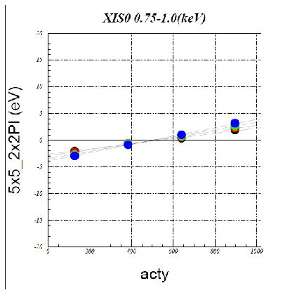 [XIS3, soft-band]
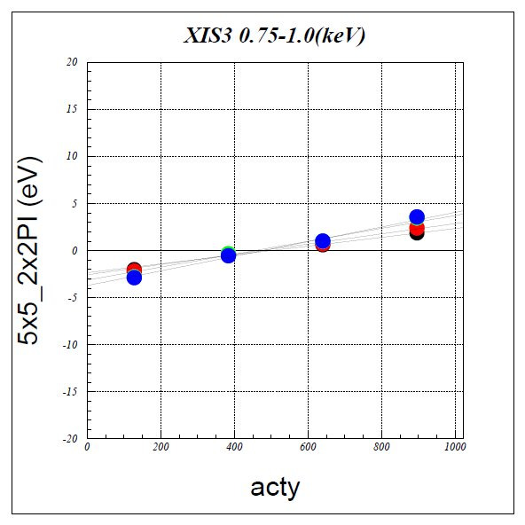 [XIS0, hard-band]
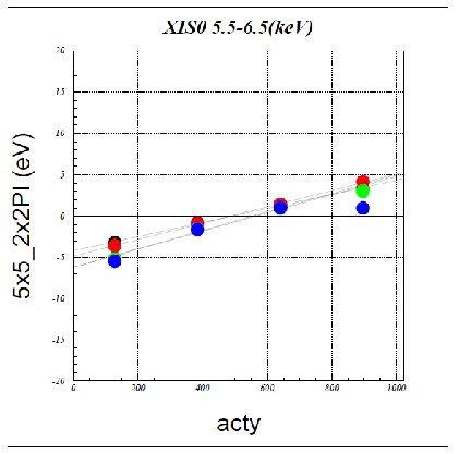 [XIS3, hard-band]
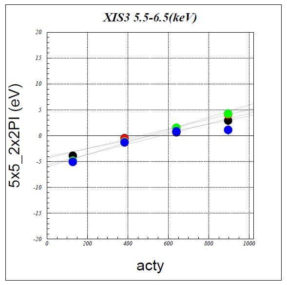
|
Users can exploit the calibration results presented above by using the xisrmfgen tool. Remaining issues include the following:
The quantum efficiency below ![]() 2keV has been decreasing since
launch due to accumulation of contaminating material on the optical
blocking filter (OBF) of each sensor. The OBF is cooler than other
parts of the satellite, thus it is prone to the accumulation of
contamination. The contaminant consists of several different materials
with time-varying composition. The time dependence of the thickness
and the chemical composition of the contaminant at the XIS nominal
position are monitored and calibrated, as well as the spatial
dependence of the thickness across the field of view (Table 7.10).
2keV has been decreasing since
launch due to accumulation of contaminating material on the optical
blocking filter (OBF) of each sensor. The OBF is cooler than other
parts of the satellite, thus it is prone to the accumulation of
contamination. The contaminant consists of several different materials
with time-varying composition. The time dependence of the thickness
and the chemical composition of the contaminant at the XIS nominal
position are monitored and calibrated, as well as the spatial
dependence of the thickness across the field of view (Table 7.10).
The chemical composition is modeled phenomenologically with
time-varying columns of H, C, N and O. Three calibration sources --
RXJ1856.5![]() 3754 (a super-soft isolated neutron star),
PKS2155
3754 (a super-soft isolated neutron star),
PKS2155![]() 304 (a blazar), and 1E0102.2
304 (a blazar), and 1E0102.2![]() 7219 (a line-dominated
supernova remnant) -- are used to derive the chemical composition at
each epoch of the observations. The spectral models by
Burwitz et al. (2003) for RXJ1856.5
7219 (a line-dominated
supernova remnant) -- are used to derive the chemical composition at
each epoch of the observations. The spectral models by
Burwitz et al. (2003) for RXJ1856.5![]() 3754, a simple power-law model for
PKS2155
3754, a simple power-law model for
PKS2155![]() 304, and the model by Plucinsky et al. (2008) for
1E0102.2
304, and the model by Plucinsky et al. (2008) for
1E0102.2![]() 7219 are used as standard
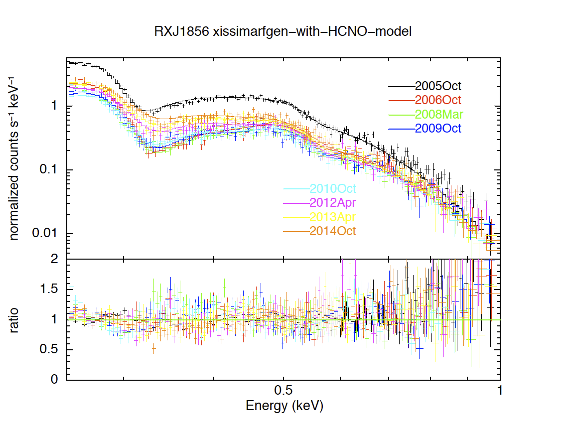
models. Fig. 7.20 shows the result of XIS1 fitting
for RXJ1856.5
7219 are used as standard
models. Fig. 7.20 shows the result of XIS1 fitting
for RXJ1856.5![]() 3754 using the 2012 contamination model for selected
epochs.
3754 using the 2012 contamination model for selected
epochs.
|
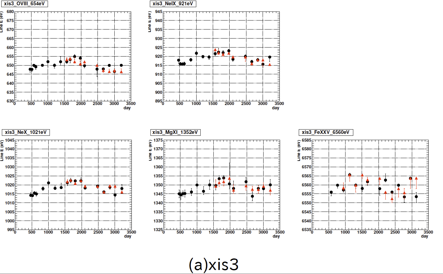
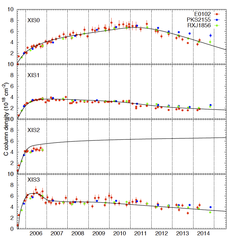
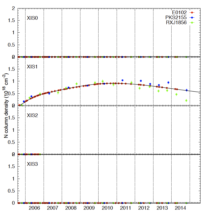
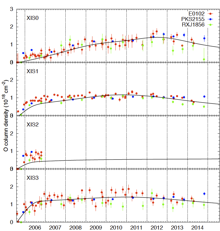
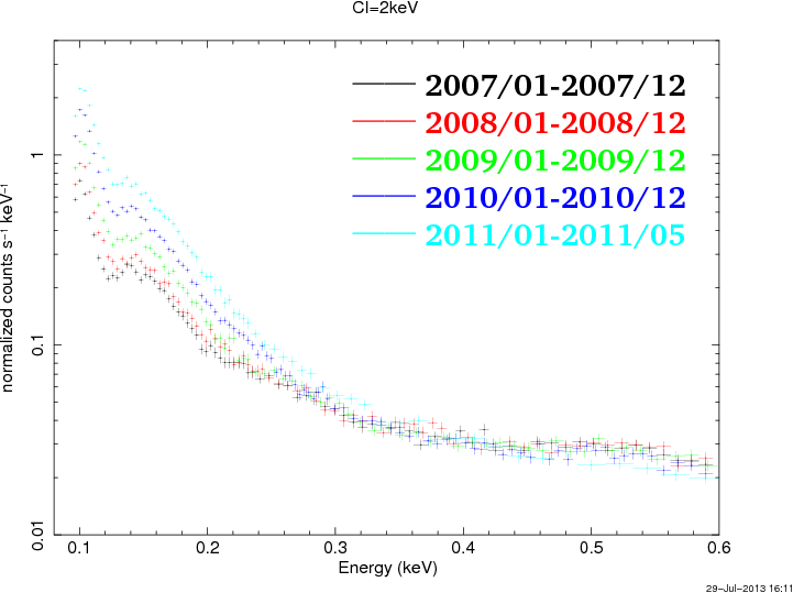
The time dependence of the thickness of the contaminant is modeled with phenomenological functions of time, separately for each composition and sensor. Fig. 7.21, 7.22, and 7.23 show the evolution of the thickness for different elements, while Fig. 7.24 shows the combined optical thickness and the relative reduction of the effective area for two different energies. The thickness increased rapidly for one year after launch and continued to increase at a moderate pace thereafter. The N component is used for the XIS1 only.
|
|
|
|
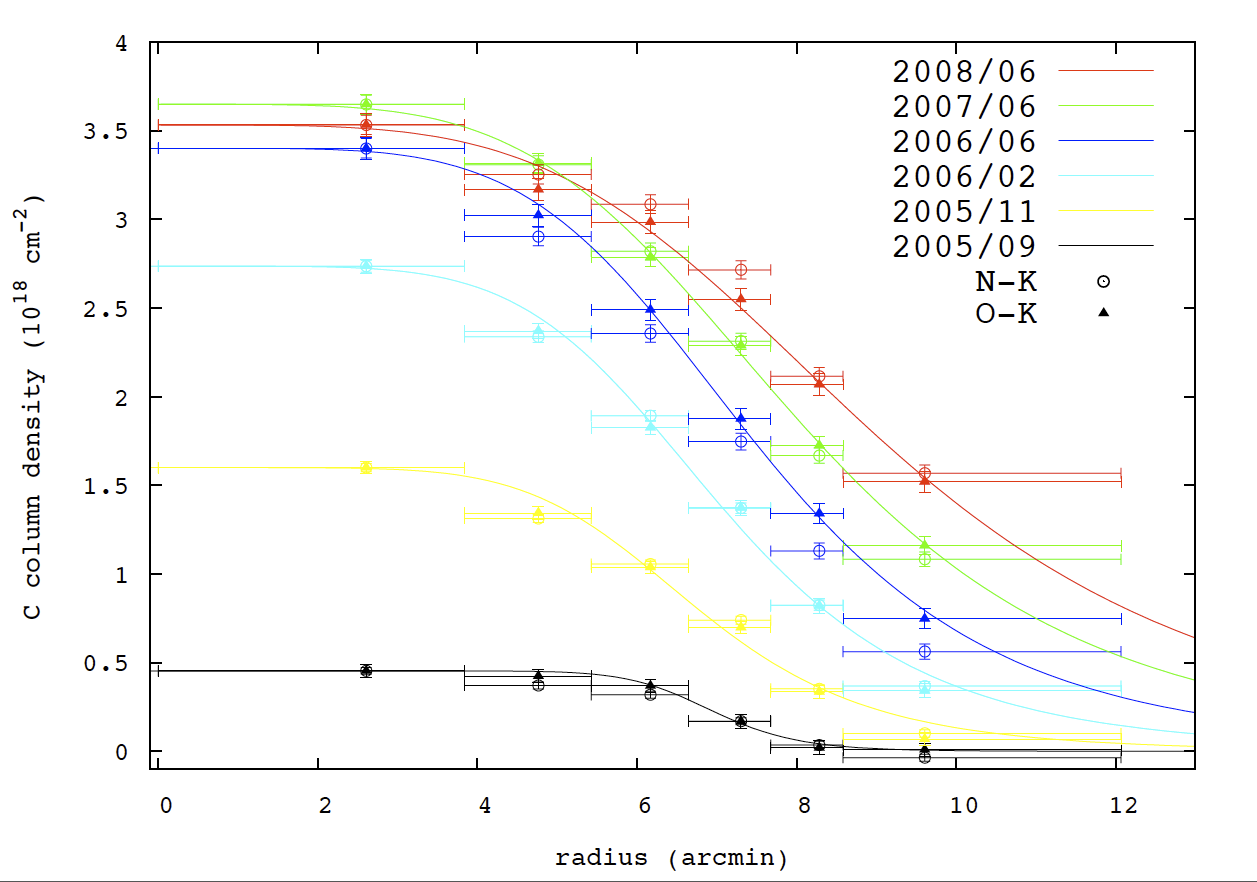
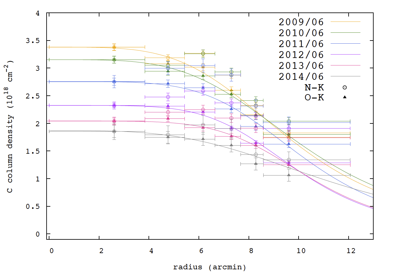
The spatial distribution of the contaminants is monitored and calibrated using regular observations of a part of the Cygnus Loop, a thermal supernova remnant. The atmospheric fluorescent K lines of N I and O I, which illuminate the entire field of view when the telescope is oriented toward the day earth, are used as well. The model of the spatial dependence assumes a radially symmetric pattern (Koyama et al., 2007). The chemical composition and the thickness at the center are normalized to the values presented in Fig. 7.21, 7.22, and 7.23. Different sensors have different radial profiles (Fig. 7.25).
|
The contaminant calibration results are available for use through the ARF generation tools xissimarfgen (Ishisaki et al., 2007) and xisarfgen. It is discouraged to use the generic contamination models in the XSPEC package (e.g., xisabs, xiscoabs, xiscoabh, xispcoab). For proposal writers ARF files are provided that assume a contamination thickness extrapolated to the middle of the next AO cycle, based on the current trend.
The Non X-ray Background (NXB) has several sources. The most dominant
source are events produced by ionization losses of charged cosmic ray
particles. Others include fluorescence X-rays from materials used in
the spacecraft and the ![]() Fe calibration sources attached to the
door of each sensor (opened immediately after the launch). Most of the
NXB events are discarded onboard as grade 7 events. The NXB of the XIS
is known to be very stable on time scales of months and thus the NXB
spectrum can be constructed using data obtained when the spacecraft is
pointed toward the Earth at night. The NXB database is accessible as
part of the CALDB, which is updated biannually in June and
December.
Fe calibration sources attached to the
door of each sensor (opened immediately after the launch). Most of the
NXB events are discarded onboard as grade 7 events. The NXB of the XIS
is known to be very stable on time scales of months and thus the NXB
spectrum can be constructed using data obtained when the spacecraft is
pointed toward the Earth at night. The NXB database is accessible as
part of the CALDB, which is updated biannually in June and
December.
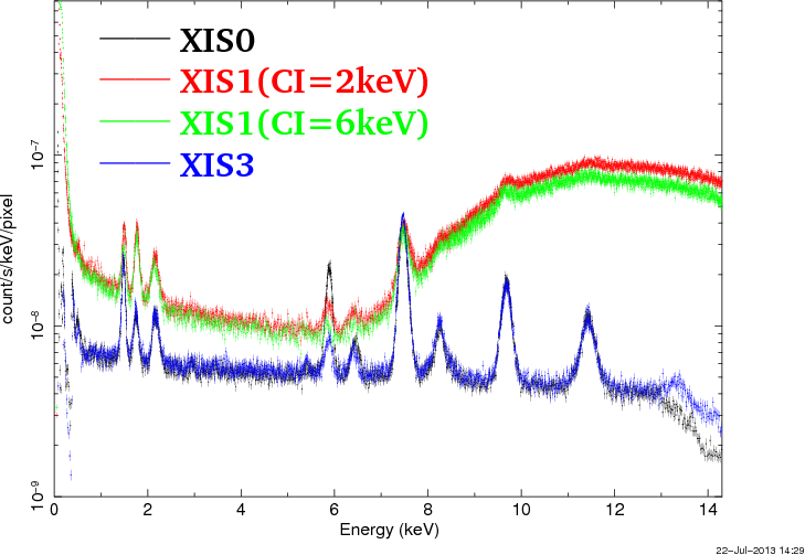
Fig. 7.26 shows the NXB spectrum for each sensor. The
background rate in the 0.4-12keV band is 0.1-0.2counts s![]() for the FI CCDs and 0.3-0.6counts s
for the FI CCDs and 0.3-0.6counts s![]() for the BI CCD after
grade selection. The background rate of XIS1 appears to become smaller
after increasing the injection charge amount from 2keV to 6keV
equivalent. The cause of this difference is currently under
investigation. Table 7.11 shows the current best estimates
for the strength of major XIS emission features, along with their 90%
confidence errors.
for the BI CCD after
grade selection. The background rate of XIS1 appears to become smaller
after increasing the injection charge amount from 2keV to 6keV
equivalent. The cause of this difference is currently under
investigation. Table 7.11 shows the current best estimates
for the strength of major XIS emission features, along with their 90%
confidence errors.
|
| Line | Energy | XIS0 | XIS1 | XIS2 | XIS3 |
| [keV] | [ |
[ |
[ |
[ |
|
| Al K |
1.486 | ||||
| Si K |
1.740 | ||||
| Au M |
2.123 | ||||
| Mn K |
5.895 | ||||
| Mn K |
6.490 | ||||
| Ni K |
7.470 | ||||
| Ni K |
8.265 | ||||
| Au L |
9.671 | ||||
| Au L |
11.51 |
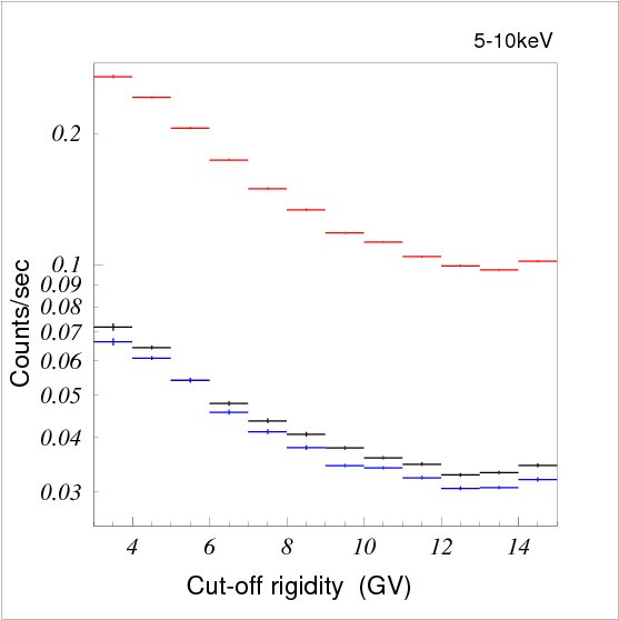
The total intensity of the NXB depends strongly on the geomagnetic
cut-off rigidity (COR), as the dominant source of the background
originates from cosmic rays. Fig. 7.27 shows the
NXB count rate as a function of the COR. The ftool
xisnxbgen generates NXB spectra for an observation
in such a way that the histogram of the COR is the same between the
observation of the source and the night Earth observations. The night
Earth data are retrieved from ![]() 150 days of the observation of the
source by default. The PIN's Upper Discriminator (PIN-UD) count rate
is also useful as a proxy for the COR, and thus the XIS NXB
level. Tawa et al. (2008) show that the PIN-UD provides a slightly better
reproducibility of the XIS NXB than the COR. The reproducibility of
the NXB in the 5-12keV band is evaluated to be 3-4% of the NXB,
when the PIN-UD is used as the NXB sorting parameter.
150 days of the observation of the
source by default. The PIN's Upper Discriminator (PIN-UD) count rate
is also useful as a proxy for the COR, and thus the XIS NXB
level. Tawa et al. (2008) show that the PIN-UD provides a slightly better
reproducibility of the XIS NXB than the COR. The reproducibility of
the NXB in the 5-12keV band is evaluated to be 3-4% of the NXB,
when the PIN-UD is used as the NXB sorting parameter.
|
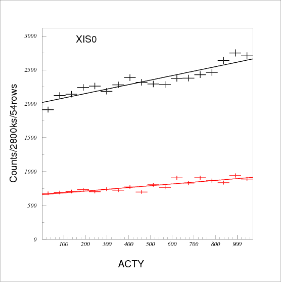
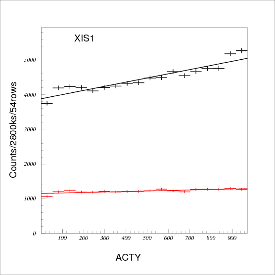
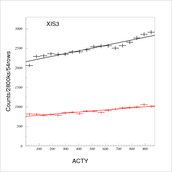
The NXB is not uniform over the chip. It is stronger toward larger ACTY positions (Fig. 7.28). This is because some fraction of the NXB is produced in the frame-store region. The fraction can be different between the fluorescent lines and the continuum.

|
The NXB level changes both continuously and discontinuously. The continuous changes are seen only in the low energy band for the BI sensor, in which a gradual increase in the NXB level is observed (Figure 7.29), although the NXB level once discontinuously decreased at the time when the injection charge was increased. The level is stable for the high energy band for the BI and the total band for the FI sensors.
|
A putative micro-meteorite hit occurred for XIS0 in 2009-06-23. Since
then, the XIS0 has been operated with an area discriminator masking
the damaged area. In the masked area, the NXB level is zero, which
causes an apparent discontinuous change in the NXB database. Users
generating their own NXB spectrum using xisnxbgen
need to be aware that they are mixing the NXB data before and after
the event if their observations are within ![]() 150 days of the event
(between January 24, 2009 and June 27, 2009). A recipe for mitigating
this is described at
150 days of the event
(between January 24, 2009 and June 27, 2009). A recipe for mitigating
this is described at
http://www.astro.isas.jaxa.jp/suzaku/analysis/xis/xis0_area_discriminaion/.
The SCI level was increased from 2 to 6keV in 2010. Due to the
increased amount of charges, the NXB level has increased
discontinuously. The increase is only seen in the second trailing rows,
which are the over-next rows from the rows with charge injection. Users
can achieve the same NXB level as for SCI![]() 2keV by masking
events from the second trailing row1s. Details can be found at
2keV by masking
events from the second trailing row1s. Details can be found at
http://www.astro.isas.jaxa.jp/suzaku/analysis/xis/xis1_ci_6_nxb/.
When the XIS field of view is close to the day Earth (i.e., Sun-lit
Earth), fluorescent lines from the atmosphere contaminate the
low energy part of the XIS data, especially for the BI chip. Most
prominent are the O and N lines. Although the standard event screening
criterion (elevation angle from the day Earth ![]() 20degrees) is
sufficient to remove these features, some emission may remain due to
the variable nature of the Earth's X-ray albedo. In this case, event
screening with a higher elevation angle is recommended.
20degrees) is
sufficient to remove these features, some emission may remain due to
the variable nature of the Earth's X-ray albedo. In this case, event
screening with a higher elevation angle is recommended.
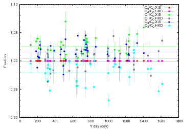
The stability of the relative normalization between the three XIS sensors is shown in Fig. 7.30. No significant change with time is found. The relative normalization remains constant. The mean and standard deviation are summarized in Table 7.12 separately for the XIS and HXD nominal positions.
|
Sudden anomalies caused putatively by micro-meteorite hits have affected XIS0, XIS1, and XIS2. The entire XIS2 was lost in 2006. A part of the XIS0 was lost in 2009, which is masked by area discrimination since then. A very small hole was created in the optical blocking filter for the XIS1, but the sensor remains intact.
The anomaly of XIS2 suddenly occurred on Nov. 9, 2006, 1:03 UT.
About 2/3 of the image was flooded with a large amount of charge,
which had leaked somewhere in the imaging region. When the anomaly
occurred, the satellite was out of the SAA and the XIS sensors were
conducting observations in the Normal mode (SCI on, without any
options). Various tests to check the condition of XIS2 revealed that
(1) the four readout nodes of the CCD and the corresponding analog
chain were all working fine, (2) the charge injection was not directly
related to the anomaly, but may have helped to spread the leaked
charge. When the clock voltages were changed in the imaging region,
the amount of leaked charge changed as well. This indicates a short
between the electrodes and the buried channel. Possible mechanisms to
cause the short include a micro-meteoroite impact on the CCD, as seen,
e.g., on XMM-Newton and Swift. Although there is no
direct evidence to indicate an micro-meteoroite impact, the phenomenon
observed for XIS2 is not very different from what is expected from such
an event. The low-earth orbit and the low-grazing-angle mirrors of
Suzaku may have enhanced the probability of a micro-meteoroite
impact. An attempt to reduce the leaked charge by changing the clock
pattern and voltages in the imaging region was not
successful. Therefore it was decided to stop operating the sensor. It
is unlikely that operation of the XIS2 will be resumed in the
future. More details can be found at
http://www.astro.isas.jaxa.jp/suzaku/doc/suzakumemo/suzakumemo-2007-08.pdf.
XIS0 suddenly showed an anomaly on June 23, 2:00 UT. During Normal
clocking operations, a part of segment A of XIS0 was flooded with a
large amount of charges, which caused saturation of the analog
electronics. The anomaly was very similar to that which occurred in
the XIS2 in 2007. It is therefore suspected that both anomalies have
the same origin, possibly a micro-meteorite impact.The effect is
confined to 1/8 of the area of XIS0. The XIS team continues to operate
XIS0. Users need to be aware of several remaining artifacts after the
event:. In the Psum clocking mode, the effect spreads to the entire
XIS0 with severe data degradation. The XIS team discontinues the use
of Psum clocking mode for the XIS0. More details can be found
at
http://www.astro.isas.jaxa.jp/suzaku/doc/suzakumemo/suzakumemo-2010-01.pdf.
XIS1 suddenly showed an anomaly some time between Dec 18, 2009 12:50
UT and 14:10 UT. A bright and persistent spot suddenly appeared at one
end of segment C in all images taken during day Earth observations,
while none was found during night Earth observations. It is speculated
that the anomaly stems from optical light leaked from a hole with a
size of ![]() 7.5
7.5![]() m in the optical blocking filter created by a
micro-meteorite hit. From diagnostic observations, it was concluded
that the scientific impact of this anomaly is minimal. XIS1 has been
and will be operated in the same way as before the anomaly. More
details can be found at
m in the optical blocking filter created by a
micro-meteorite hit. From diagnostic observations, it was concluded
that the scientific impact of this anomaly is minimal. XIS1 has been
and will be operated in the same way as before the anomaly. More
details can be found at
http://www.astro.isas.jaxa.jp/suzaku/doc/suzakumemo/suzakumemo-2010-03v2.pdf.
We obtained some frame dump images of the day Earth in 2013, July 16,
and found a total of 10 new bright spots on XIS1 and XIS3. We
speculate that they are caused by OBF holes for their similarities
with the event in 2009 December for XIS1. The sizes of the OBF holes
are estimated to be very small, ![]() 0.3 pixels, so they are expected
to have no effect on the X-ray data unless an optically bright source
coincidently falls onto one of the holes. More details can be found
at
0.3 pixels, so they are expected
to have no effect on the X-ray data unless an optically bright source
coincidently falls onto one of the holes. More details can be found
at
http://www.astro.isas.jaxa.jp/suzaku/doc/suzakumemo/suzakumemo-2013-01.pdf.
When a CCD pixel absorbs an X-ray photon, the X-ray is converted to an electric charge, which in turn produces a voltage at the analog output of the CCD. This voltage (``pulse height'') is proportional to the energy of the incident X-ray. In order to determine the true pulse height corresponding to the input X-ray energy, it is necessary to subtract the dark levels and correct possible optical light leaks.
Dark levels are non-zero pixel pulse heights caused by leakage currents in the CCD. In addition, optical and UV light might enter the sensor due to imperfect shielding (``light leak''), producing pulse heights that are not related to X-rays. The analysis of ASCA SIS data, which utilized an X-ray CCD in photon-counting mode for the first time, showed that the dark levels were different from pixel to pixel, and the distribution of the dark level did not necessarily follow a Gaussian function. On the other hand, light leaks are considered to be rather uniform over the CCD.
For the Suzaku XIS, the dark levels and the light leaks are calculated separately in the Normal mode. The dark levels are defined for each pixel and are expected to be constant for a given observation. The PPU calculates the dark levels in the Dark Initial operation; those are stored in the Dark Level RAM. The average dark level is determined for each pixel, and if the dark level is higher than the hot-pixel threshold, this pixel is labeled as a hot pixel. The dark levels can be updated by the Dark Update operation, and sent to the telemetry by the Dark Frame mode. The analysis of ASCA data showed that the dark levels tend to change mostly during the SAA passage of the satellite. The Dark Update operation is conducted after every SAA passages unless the telescope is pointed toward the day Earth.
Hot pixels are pixels which always output pulse heights larger than the hot-pixel threshold even without input signals. Hot pixels are not usable for observations, and their output has to be disregarded during scientific analysis. The XIS detects hot pixels on-board by the Dark Initial/Update mode, and their positions are registered in the Dark Level RAM. Thus, hot pixels can be recognized on-board, and they are excluded from the event detection processes. It is also possible to specify hot pixels manually. However, some pixels output pulse heights larger than the threshold intermittently. Such pixels are called flickering pixels. It is difficult to identify and remove flickering pixels on board. They are inevitably included in the telemetry and need to be removed in scientific analysis, for example by using the FTOOLS sisclean. Flickering pixels sometimes cluster around specific columns, which makes them relatively easy to identify.
The light leaks are calculated on board from the pulse height data
after subtraction of the dark levels. A truncated average is
calculated for ![]() pixels (this size was
pixels (this size was ![]() before January 18, 2006) in every exposure and its running average
produces the light leak. In spite of the name, light leaks do not
represent in reality optical/UV light leaks in the CCD. They mostly
represent fluctuation of the CCD output correlated to the variations
of the satellite bus voltage. The XIS has little optical/UV light
leak,it is negligible unless the bright earth comes close to the XIS
field of view.
before January 18, 2006) in every exposure and its running average
produces the light leak. In spite of the name, light leaks do not
represent in reality optical/UV light leaks in the CCD. They mostly
represent fluctuation of the CCD output correlated to the variations
of the satellite bus voltage. The XIS has little optical/UV light
leak,it is negligible unless the bright earth comes close to the XIS
field of view.
The dark levels and the light leaks are merged in the Parallel-sum (P-Sum) mode, so the Dark Update mode is not available in the P-Sum mode. The dark levels, which are defined for each pixel as in the case of the Normal mode, are updated every exposure. It may be considered that the light leak is defined for each pixel in the P-Sum mode.
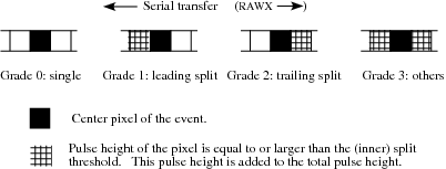
The main purpose of the on-board processing of the CCD data is to reduce the total amount of data transmitted to the ground. For this purpose, the PPU searches for a characteristic pattern of the charge distribution (called an event) in the pre-processed (post dark level and light leak subtraction) frame data. When an X-ray photon is absorbed in a pixel, the photo-ionized electrons can spread into at most four adjacent pixels.
An event is recognized when a pixel has a pulse height which is
between the lower and the upper event thresholds and is larger than
those of eight adjacent pixels (e.g., it is the peak value in the
![]() pixel grid). In the P-Sum mode, only the horizontally
adjacent pixels are considered. The copied and the dummy pixels ensure
that the event search is enabled on the pixels at the edges of each
segment. The RAW XY coordinates of the central pixel are considered
the location of the event. Pulse-height data for the adjacent
pixel grid). In the P-Sum mode, only the horizontally
adjacent pixels are considered. The copied and the dummy pixels ensure
that the event search is enabled on the pixels at the edges of each
segment. The RAW XY coordinates of the central pixel are considered
the location of the event. Pulse-height data for the adjacent ![]() square pixels (or three horizontal pixels in the P-Sum mode)
are sent to the Event RAM as well as the pixel location.
square pixels (or three horizontal pixels in the P-Sum mode)
are sent to the Event RAM as well as the pixel location.
The MPU reads the Event RAM and edits the data to the telemetry
format. The amount of information sent to the telemetry depends on the
editing mode of the XIS. All the editing modes are designed to send
the pulse heights of at least four pixels of an event to the
telemetry, because the charge cloud produced by an X-ray photon can
spread into at most four pixels. Information of the surrounding pixels
may or may not be output to the telemetry depending on the editing
mode. The ![]() mode outputs the most detailed information to the
telemetry, i.e., all 25 pulse-heights from the
mode outputs the most detailed information to the
telemetry, i.e., all 25 pulse-heights from the ![]() pixels
containing the event. The size of the telemetry data per event is
reduced by a factor of two in the
pixels
containing the event. The size of the telemetry data per event is
reduced by a factor of two in the ![]() mode, and another factor
of two in the
mode, and another factor
of two in the ![]() mode. Details of the pulse height information
sent to the telemetry are described in the next section.
mode. Details of the pulse height information
sent to the telemetry are described in the next section.
Three kinds of discriminators, area, grade, and class discriminators, can be applied during the on-board processing. The grade discriminator is available only in the Timing mode. The class discriminator was implemented after the launch of Suzaku and was used since January, 2006. In most cases, guest observers need not change the default setting of these discriminators.
The class discriminator classifies the events into two classes,
``X-rays'' and ``others,'' and outputs only the "X-ray" class to the
telemetry when it is enabled. This class discriminator is always
enabled to reduce the telemetry usage of non-X-ray events. The
``other'' class is close to, but slightly different from the ASCA
grade 7. When the XIS points to a blank sky, more than 90% of the
detected events are particle events (mostly corresponding to ASCA
grade 7 events). If we reject these particle events on board, we can
make a substantial saving in the telemetry usage. This is especially
useful when the data rate is medium or low. The class discriminator
realizes such a function in a simple manner. When all the eight pixels
surrounding the event center exceed the Inner Split Threshold, the
event is classified as from the ``other'' class, and the rest of the
events as from the ``X-ray'' class. With such a simple method, we can
reject more than three quarters of the particle events. The class
discriminator works only for the ![]() and
and ![]() modes. It is not available in the
modes. It is not available in the ![]() mode and the timing
mode.
mode and the timing
mode.
Fig. 7.5 shows the pixel pattern for which the pulse
height or 1-bit information is sent to the telemetry. We do not assign
grades to an event on board in the Normal Clock mode. This means that
a dark frame error, if present, can be corrected accurately during
ground processing even in the 2 ![]() 2 mode. The definition of the
grades in the P-Sum mode is shown in Fig. 7.31.
2 mode. The definition of the
grades in the P-Sum mode is shown in Fig. 7.31.
|
![\begin{landscape}
% latex2html id marker 2868\begin{table}[hp]
\centering
\...
...ased for damaged area.\\
%
\hline
\end{longtable} \end{table}\end{landscape}](img149.png)
![\begin{landscape}
% latex2html id marker 3212\begin{table}[p]
\centering
\c...
...d{footnotesize} \end{tablenotes} \end{threeparttable} \end{table}\end{landscape}](img188.png)