Next: 7. Spatial-Spectral Mixing: Extended Up: xrism pog Previous: 5. Resolve Contents
Xtend is the soft X-ray imaging telescope of XRISM , with a pair of X-ray mirrors
(X-ray Mirror Assemby: XMA, Tamura et al., 2024) and
an X-ray CCD imaging spectrometer (Soft X-ray imager: SXI, Noda et al., 2025).
Xtend has a larger field of view (38.5 38.5
38.5 ) and a low/stable non-X-ray background, ideal for
observing diffuse X-ray emission with low surface brightness.
The large field of view (FOV) and the finer pixel size (1.77
 ) also provide more detailed spatial information
of or around the target, extending the capabilities of Resolve's spectroscopy by evaluating contamination from sources outside
Resolve's FOV and measuring the local diffuse background (Figure 6.1).
Xtend works in a complementary role to Resolve.
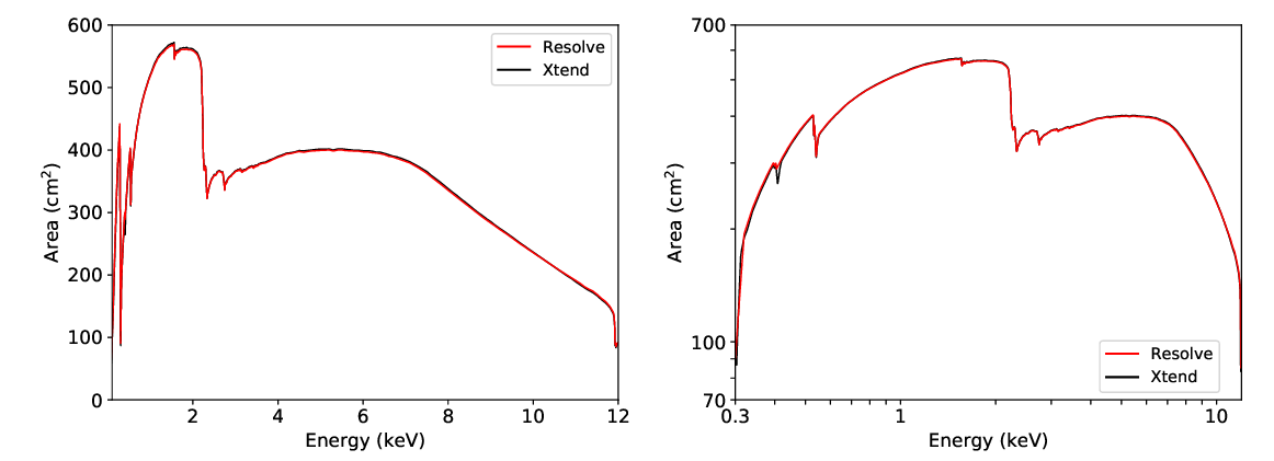
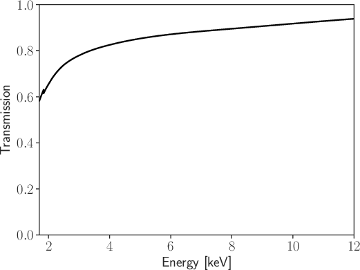
Besides a few improvements, Xtend is almost identical to the Astro-H SXT + SXI telescope system (see Section 6.4.7). Therefore, its publications and archival data should be a good reference for Xtend 's performance (Uchida et al., 2025; Noda et al., 2025). This chapter describes the SXI module and the combined performance of the XMA and SXI. Chapter 4 describes the XMA-specific performance, which has an identical design to Resolve's XMA telescope but with a slightly different performance.
![\begin{figure}\centering
\includegraphics[width=0.9\textwidth]{Figures_Xtend/xtend_image.pdf}\end{figure}](img105.gif) |
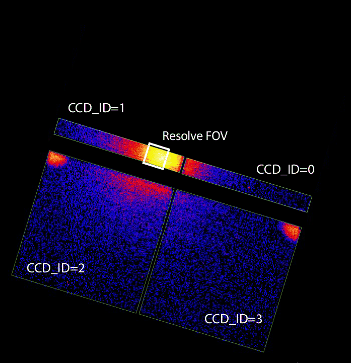
The SXI houses four identical X-ray CCD sensors in a 2 2 grid.
Each CCD has an identifier, CCD_ID=0
 3,
used for the science and housekeeping data
(Figure 6.2). (Note that the instrument team and manufacturer also uses another identifier CCD1-4,
which has the same numbering order but starts from 1 (e.g., CCD1 for CCD_ID=0). This document consistently uses the CCD_ID identifier to avoid confusion.)
These CCDs are similar to those on earlier or ongoing X-ray observatory missions,
such as Suzaku XIS, Chandra ACIS, and XMM-Newton EPIC-MOS.
However, the SXI CCDs utilize the p-channel, backside-illumination technology, which realizes
a thick depletion layer of 200
  m, with high quantum efficiencies in a broad energy range between 0.4
 13 keV.
The following list describes the key instrument performance. Table 6.1 also summarizes Xtend 's characteristics.
![\begin{figure}\centering
\includegraphics[width=0.9\textwidth]{Figures_Xtend/fig_Xtend_CCD_v10.pdf}\end{figure}](img107.gif) |
| Field of View | 38.5  38.5 38.5 (Full window) (Full window) |
| Sensitive band | 0.4  13 keV 13 keV |
| Effective area | 420 cm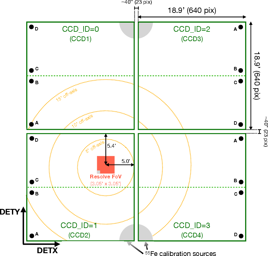 @1.5 keV, 310 cm @1.5 keV, 310 cm @6 keV @6 keV |
On-axis XMA PSF at 6.4 keV
 |
1.4 (HPD), 7.2 (HPD), 7.2 (FWHM) (FWHM) |
| Pixel size | 1.77 (48 (48 m, logical) m, logical) |
| Time resolution | 4 sec (Full window), 0.5 sec (1/8 window) |
| Energy resolution (FWHM) |  170 170 180 eV @ 6 keV 180 eV @ 6 keV |
| Pileup tolerance | 2.5 mCrab (Full window) |
| Total (NXB + Sky) X-ray background | 1.5 10 10 counts s counts s keV keV arcmin arcmin cm cm |
| HPD: Half Power Diameter. | |
 See the XMA chapter (4) for the details. See the XMA chapter (4) for the details. |
|
| These values are based on ground or in-flight calibrations. | |
| Reference: Table 1 and Figure 20 in Uchida et al. (2025). | |
Field of View: The 2 2 CCD array covers a 38.5
 38.5
38.5 square FOV with small mechanical gaps between the CCD chips.
The gaps between the active pixel regions are 44
 59
59 (1.2
(1.2 1.6 mm).
The aimpoint co-aligns with the Resolve aimpoint and offsets by 4.7
 and 4.7
 from the CCD edges
of CCD_ID=1 to avoid the chip gap.
In the 1/8 window mode,
the 2 CCDs (CCD_IDs 0 and 1) have a narrow rectangular FOV with the aimpoint at the center of the widths.
The long side does not touch the CCD edges,
having a relatively big imaging gap with the other 2 CCDs' FOV (Figure 6.5, Section 6.2).
Sensitive Energy Range & Quantum Efficiency:
The SXI CCD sensors have a p-type channel and n-type substrate, enabling a thick depletion
layer of  200
200  m and realizing a large X-ray stopping power up to
  13 keV.
They are backside illuminated CCDs with high transparency to soft X-rays.
The SXI system also has the Optical Blocking Layer (OBL) on the CCD surface to block optical/IR lights and
the Contamination Blocking Filter (CBF) at the hood top to avoid molecular contamination build-up and further block optical/IR lights.
These components limit the soft X-ray sensitivity to
  0.4 keV.
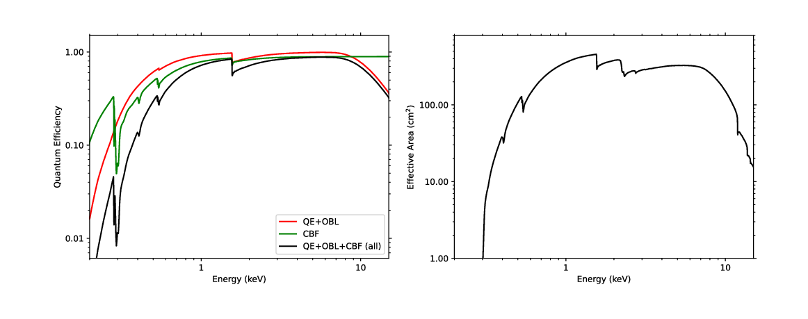
Figure 6.3 left shows the SXI CCD quantum efficiency.
Effective Area: This value primarily depends on the XMA's collecting area (see Section 4.2.2) and the
CCD's quantum efficiency.
In addition, the SXI runs with the charge injection operation through the mission,
which produces 1 3 insensitive CCD rows every 80 rows and reduces the sensitive area by 1
 3%.
Figure 6.3 right shows the effective area of the entire Xtend system for a point source at the on-axis position.
The effective area may decline due to radiation damage to CCD pixels or contamination condensing on the mirror or filter during operation.
The instrument and science operations teams will calibrate and update the value in the calibration database regularly.
Angular Resolution: Each CCD has a square imaging area with 1280 1280 physical pixels,
each 24
  m long, which are binned by 2 pixels onboard for science observations.
Therefore, the output science data have 640
 640 “logical" pixels, each 48
  m in length,
equivalent to 1.77
 in the sky.
This pixel size is significantly smaller than the on-axis PSF's half-power diameter (1.47
 )
and FWHM (7.2
 ) (see Chapter 4).
![\begin{figure}\begin{center}
\includegraphics[width=0.9\textwidth]{Figures_Xtend/fig_xtend_qe_eff.pdf}\end{center}\end{figure}](img111.gif) |
Time resolution: The nominal operation (the Full window mode without the burst option, see Section 6.2)
takes a frame exposure for 3.96 seconds
and transfers charge produced by X-ray or particle events during the exposure
to the shielded frame store area in 36.864 milliseconds for readout.
The imaging area takes another exposure right after this transfer.
This operation continuously collects data every 4 seconds and has a 4-second
fixed time resolution.
The 1/8 window mode without the burst option runs the same cycle but only in 0.5 seconds,
with a short  0.46-second frame exposure and a readout of a small 1/8 window area.
The mode, therefore, has a 0.5-second continuous time resolution.
The 1/8 window mode without the burst option runs a similar cycle but only in 0.5 seconds,
with a short
  0.46 sec frame exposure and a readout of a small 1/8 window area.
The mode, therefore, has 0.5-second continuous time resolution.
The 1/8 window mode with the 0.1 s burst option also has a similar cycle but with
a 0.062 second frame exposure.
A readout still takes
  0.5 seconds, so most of which is deadtime,
and the data are collected every 0.5 second.
However, each frame exposure has better time precision with a narrow exposure,
which should help constrain pulse period measurements.
Energy resolution: The CCD energy resolution depends on the statistical fluctuation of charges
produced by X-ray photons, the number of charges lost during the CCD charge transfer
(charge transfer inefficiency: CTI), and the readout electric noise.
Normally, the first component, charge statistical fluctuation, is the most significant factor in the CCD energy resolution.
Higher energy X-rays have worse absolute energy resolution ( ) with
more charges but better relative energy resolution (
 /
/ ) with better statistics.
An in-orbit calibration verified the energy resolution of 170
 180 eV at 5.9 keV (FWHM).
The CTI normally gets worse through the mission with in-orbit radiation damage.
The instrument and science operations teams will calibrate the energy resolution regularly with the
  Fe calibration sources and/or
celestial source observations and updates the result in the calibration database.
Background:
Cosmic Ray (CR) particles or fluorescent X-rays from detector materials excited by those particles
interact with the CCD sensors and produce charge clouds in CCD pixels.
The grade selection method effectively excludes those events but cleaned data still include some
particle events called Non-Xray Background (NXB).
The NXB flux varies on a short timescale with the satellite orbit, correlating well with
the Cut-Off Rigidity (COR) value,
and on a long timescale with the 11-year Solar cycle
(Figure 6.4 left, Uchida et al., 2025).
The amount of NXB depends on the exposed duration of each pixel on a CCD and, therefore, the CCD rows (i.e., vertical frame transfer direction).
The instrument and science operations teams have been studying the contribution of NXB to cleaned data
in various observatory environments.
The sky background
contribution should be 1.5 10
10 counts s
 keV
keV arcmin
 cm
cm in the 5
 10 keV band,
similar to the Hitomi SXI (Figure 6.4 right, Uchida et al., 2025).
We provide an instruction and relevant tools to evaluate the NXB spectra during individual observations from the PV and Cycle 1 data and template spectrum for the Cycle 3 proposal at
https://heasarc.gsfc.nasa.gov/docs/xrism/proposals/responses.html.
![\begin{figure}\centering
\includegraphics[width=0.9\textwidth]{Figures_Xtend/xtend_spec_background.pdf}\end{figure}](img114.gif) |
Users can choose the following optional operation modes for CCD_ID=0 and 1 to observe bright sources and/or improve time resolution (Table 6.2). These two sensors run in the same mode as they share the CCD sequences, while the CCD_ID=2&3 sensors always run with the Full window mode.
![\includegraphics[totalheight=3in]{Figures_Xtend/xtend_image_oneeighth.pdf}](img115.gif)
|
 |
Image Size | Time Res. | Exp. time | LTF | Pile-up | |
(H)  (V) (V) |
(sec) | (sec) | (mCrab) | |||
| Full Window No Burst | 1 | 640 640 640 |
4 | 3.9631 | 0.99 | 2.5 |
| 1/8 Window No Burst | 8 | 640 80 80 |
0.5 | 0.4631 | 0.93 | 21 |
| 1/8 Window 0.1s Burst | 8 | 640 80 80 |
0.5
 |
0.0620 | 0.12 | 160 |
 : Number of exposure in a unit time interval (4 sec). : Number of exposure in a unit time interval (4 sec). |
||||||
| Image Size: each CCD chip size. | ||||||
| LTF: Live Time Fraction. | ||||||
Pile-up: On-axis source flux that suffers 10% photon pile-ups, equivalent to an SXI count rate at 6.3 cts s . . |
||||||
 Users can measure each photon's arrival time information with Users can measure each photon's arrival time information with  0.06 sec accuracy. 0.06 sec accuracy. |
||||||
Many point sources optimal for Resolve observations would exceed the Full window mode pileup limit. Even some diffuse sources like Perseus cluster, Pup A and Cas A have bright knots that go beyond the pileup limit (see e.g., Figure 3 in Tsunemi et al., 2013). Which Xtend mode should users choose?
The answer depends on the goal of their Xtend observation.
If users want to collect as many photons as possible, from only the aimpoint target,
they should choose the 1/8 window mode and add the burst option if the target is brighter than  21 mCrab.
However, the pileup occurs only near the PSF core,
so users may be able to utilize data from the extended PSF outskirts with little photon pileups using the Full window mode.
The HEASOFT tool, pileest, would help estimate pileup fraction from obtained event data.
Two or more X-ray photon events are indistinguishable when they fall in 3 3 CCD pixels in a single frame exposure;
such an incident is called photon pileup (Yoneyama et al., 2025).
Many pileup events have two photons at different pixels, recognized as a multiple-pixel event and discarded,
while others are just counted as single X-ray events.
Either way, the SXI counts two or more pileup X-ray photons as one or zero,
underestimating the photon flux.
If detected as single X-ray events, pileup events have an energy of two or more X-ray photons,
making the spectrum harder.
The PSF core has the highest count rates per CCD pixel and prone to pileup.
The PSF peak diminishes as the source flux increases and turns into a hole in a severe case.
The pileup fraction is the ratio of pileup events over all incoming X-ray events.
Xtend SXI reaches the 10% pileup limit at a count rate of 6.3 cts s , corresponding to
  4.5
4.5 10
10 ergs cm
 s
s between 2
 10 keV
for the Crab nebula spectrum with a power-law
  at 2.13 (an IACHEC model; see https://iachec.org).
Pileup tolerance depends on users' science goals.
For example, users should minimize the pileup to detect a weak hard spectral tail, while they may allow some degree of pileups to detect emission lines.
Out-of-time events are X-ray events detected during the CCD frame transfer — parallel transfer of charges from
the imaging area to the frame store area.
One logical pixel transfer takes only 57.6  sec, so only bright sources appear as vertical streaks above the background in images.
Out-of-time events rarely suffer photon pileups as detected charges stay in a fraction of time in a pixel,
and so can be used for measuring non-pileup spectra of extremely bright sources.
In the normal clocking mode, out-of-time events constitute a uniform brightness streak and contribute
only  0.93% of the total counts from a target.
In the burst option, they constitute a significant fraction of the source counts with a relatively long frame transfer
interval to the frame exposure, contributing 7.3% of the source count during the exposure.
Very bright sources create so many X-ray events that their charges also work as fillers of charge traps in the CCD chips (Todoroki et al., 2012; Kanemaru et al., 2020). This effect improves the spectral resolution, but it depends on the source brightness and is difficult to estimate. The instrument team does not plan to implement the effect in the standard calibration.
The following sections describe the detail of the SXI instrument. They may not necessarily be for proposal preparation, but they should help understand how the instrument works.
The SXI sensor (SXI-S) is placed at one of the two XMA's focal plane — 5.6 m below the mirror — on the XRISM's optical bench.
The SXI instrument system consists of four components:
a sensor body (SXI-S), pixel processing electronics (SXI-PE), digital electronics (SXI-DE), and a cooler driver (SXI-CD).
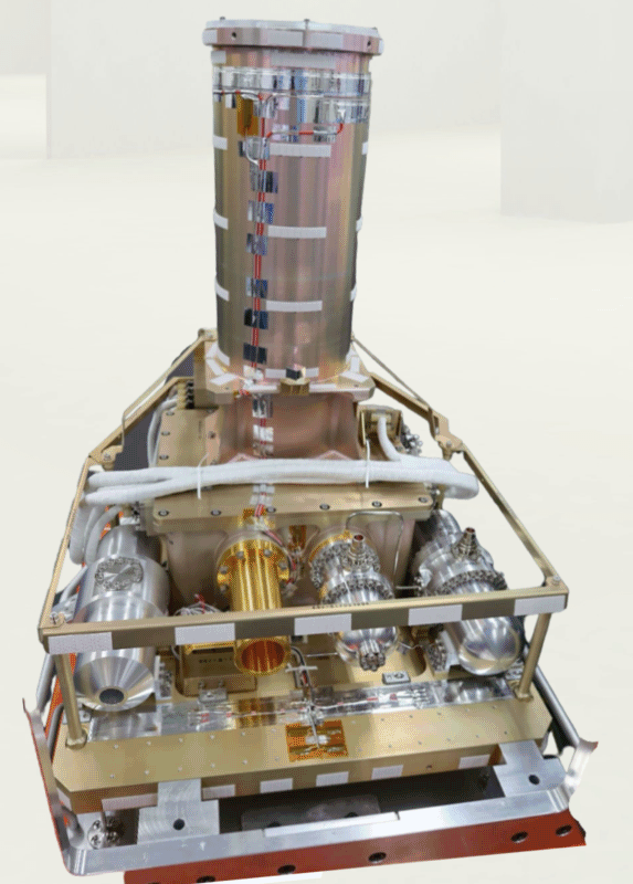
The SXI-S (Figure 6.6)
includes the CCDs and their supporting systems, driver and video electronics, a single-stage Stirling cooler, and calibration sources.
The SXI-PE extracts X-ray event information from initial image data.
The SXI-DE packages X-ray event and associated housekeeping (HK) data
and delivers them to the Satellite Management Unit (SMU).
The SXI-DE controls the Stirling cooler and associated heater, keeping the CCD sensor's temperature
at  110
110  C (early operational phase),
  120
120  C (late phase), or required temperatures.
| CCD Type | Frame transfer,  -channel, Backside illumination -channel, Backside illumination |
| Number of CCDs | 4 |
| Number of segments per CCD | 2 |
| Imaging area | 31 31 mm 31 mm , 640 , 640 640 logical pixels 640 logical pixels |
(1280 1280 physical pixels) 1280 physical pixels) |
|
| Pixel size | 24  m m 24 24  m (physical pixels) m (physical pixels) |
| CCD gap | 1.2 1.6 mm (44 1.6 mm (44 59 59 ) ) |
| Depletion depth | 200  m m |
| Optical blocking layer | Al(100 nm)/Al(100 nm) deposited on the CCD surface |
| Contamination Blocking Filter | Al(80nm)/Polyimide(200nm)/Al(40nm) |
| CCD operating temperature |  110 110  C/ C/ 120 120  C C |
| Calibration sources | two  Fe radioisotopes Fe radioisotopes |
Hamamatsu Photonics K.K. fabricated twelve flight-model candidate CCD chips,
and the Xtend team selected four CCD flight-model chips among them (Yoneyama et al., 2021).
The SXI CCDs have a  -type channel and
  -type substrate, in which positively charged holes act as mobile charge
carriers instead of electrons for earlier X-ray CCD cameras (See Figure 1 in Bebek et al. (2004)).
The high resistivity of the
  -type substrate produces a thick depletion layer so that
the CCDs are fully depleted to the back surface with a depth of
  200
200  m.
For comparison, the Suzaku XIS backside illuminated CCD with a
  -type Si substrate was polished to 45
  m to ensure full depletion.
The large SXI CCD depletion depth combined with the backside illumination improves the quantum efficiency
at both soft and hard X-ray energies.
The larger depletion depth causes longer drift length and more extensive diffusion.
This effect strongly affects soft X-ray photons absorbed near the CCD surface:
because the CCDs are backside illuminated, their charges need to drift from near the surface to the bottom with the electrodes.
X-ray event charges rarely fall in a single physical CCD pixel (24  m
m 24
24  m) but multiple pixels.
To simplify the event processing, the SXI nominally combines charges in every set of 2
 2 original pixels
before the CCD readout and converts them to a digital value.
This 2
 2 onboard binning format has
  30% of X-ray events in a single binned pixel,
and the rest within 3
 3 binned pixels.
In the following, the "physical" pixel refers to the original 24
  m
m 24
24  m CCD pixel,
while the "logical" pixel does the 2
 2 binned 48
  m
m 48
48  m, pixel.
The SXI science data output in the 640
 640 logical pixel format for each CCD.
Each CCD chip has a rectangular shape with a square imaging area (IA) and frame store (FS) area.
The IA has 1280 1280 physical pixels, exposed to the sky through the XMA for X-ray photon detection.
The FS also has 1280
 1280 pixels but is covered with a metal plate and used solely for temporary charge storage.
In a normal data acquisition sequence (Figure 6.7), the IA detects X-ray photons in a frame exposure
(3.96 sec in the normal clocking, Full window mode),
whose charges quickly drift to the buried channel of the corresponding pixels.
After the exposure, the CCD clock driver changes the electrode voltages (so-called clocking)
to move the accumulated charges by one vertical pixel at one cycle
and repeat this cycle 1280 times to transfer all charges in IA to FS.
This “parallel transfer" process transfer all charges in the 1280 CCD columns in parallel.
One pixel shift takes 28.8
  sec, and a whole parallel transfer from IA to FS takes 36.9 msec.
During each parallel transfer, the SXI also operates charge injection
for the subsequent frame exposure (Section 6.4.2 for the detail)
so that the parallel transfer duration depends on the charge injection frequency and the clocking mode
After the parallel transfer, the CCD driver transfers charges in the bottom row horizontally to readout nodes with two serial registers. A serial register handles a CCD segment, moving charges in the bottom row by one horizontal pixel at one clock cycle toward the active readout node. An analog-to-digital converter measures the number of charges at the readout and stores the value in memory. Once the serial register reads charges in the whole pixels in the horizontal line, the driver vertically transfers all FS charges by one pixel and then read charges moved to the bottom row. The driver continues this sequence until reading all FS charges.
![\begin{figure}\centering
\includegraphics[totalheight=2in]{Figures_Xtend/fig_xtend_charge_transfer_HitomiTD.pdf}\end{figure}](img121.gif) |
Defects in the CCD silicon lattice can hold charges for a short time. If a defect, or so-called trap, is on an electrode, it can capture a portion of charges under transfer and keep them until untrapped charges move to a downward pixel. This process, called charge transfer inefficiency or CTI, occurs stochastically, producing a tail to the original charge distribution and adding noise to the reconstructed event pulse height. The chance of trap increases with the number of pixel transfers, so more charges tend to be ripped off from events detected further from the readout node (i.e., large RAWY coordinates). The SXI chips have relatively large CTIs in the ground testing, and the CTI is expected to progress in orbit as particles continuously bombard CCDs and break the silicon lattice (Kanemaru et al., 2019).
To ameliorate the CTI problem, the SXI employs the charge injection (CI) technique.
The Suzaku observatory's X-ray CCD camera (XIS) employed this technique for the first time in orbit and substantially improved
the energy resolution in the middle of the mission to near the initial performance (see, for example, Bautz et al., 2007; Uchiyama et al., 2009).
This technique artificially fills a large number of charges every  CCD row, which fill traps before X-ray events
pass the traps during the vertical transfer (Figure 6.7).
Figure 6.8 clearly shows that the calibration source spectra improves with the CI operation.
A downside is that the CI rows stay in the IA during frame exposures, so these lines, and probably their leading and trailing rows,
cannot detect X-rays.
This limitation reduces the effective area by 1/
 or more.
Most trapped charges escape quickly and appear in a few trailing pixels.
These charges change the original 5 5 pixel patterns, which is problematic for the grade event extraction classification.
This charge migration can be statistically estimated and restored, and so
the charge trail correction algorithm runs during the pipeline processing to fix the problem.
A small amount of charges reappear outside the 5
 5 pixels, causing an artificial pulse height deficit.
The CTI correction algorithm in the pipeline processing (Kanemaru et al., 2020) recovers the expected loss
based on the ground and onboard calibration study (Uchida et al., 2025; Yoneyama et al., 2020).
![\begin{figure}\centering
\includegraphics[width=0.9\textwidth]{Figures_Xtend/fig_xtend_w_wo_CI_HitomiTD.pdf}\end{figure}](img122.gif) |
The readout wire of each Xtend CCD segment has electric crosstalk with that of the paired segment. When a cosmic ray hits a CCD pixel and produces significant charges in that pixel, the corresponding pixel of the paired segment receives a weak, opposite (i.e., negative) crosstalk signal during the readout. The onboard software considers the signal as a change in the pixel's pedestal (or dark) signal level and reduces the dark level for the following frame exposures. If this decline is significant, the pixel outputs a net signal above the event threshold without an actual charge signal. It wrongly detects an event at every frame exposure after the cosmic ray event. Since cosmic rays constantly hit CCDs, crosstalk pixels increase steadily during observation until the instrument resets the dark level after one day.
Crosstalk events appear mainly in the outer segments; almost none are near the on-axis.
They mostly have pulse heights equivalent to energies below 0.4 keV, but some do up to  0.6 keV.
Thus, analysis of soft X-ray spectra below
  0.6 keV, off-axis sources, or extended sources requires careful inspections of crosstalk event contaminations. Note that the current (as of January 2026) non-X-ray
background archival data exclude these events using the 'searchflickpix' tool (see below), but not perfectly.
The XRISM Science Data Center (SDC) outlines a method for effectively reducing cosmic-ray echo events using the 'xtdpixclip' tool in the XRISM quick-start guide, which allows users to manually set an event-count threshold for a dataset using a histogram and remove events from pixels above that threshold. The Xtend team is also developing a dedicated tool that recovers actual X-ray events detected on crosstalk pixels for data analysis.
Defects in the CCD silicon lattice can also produce charge currents without X-ray or particle events, which appear as high pulse height pixels called hot pixels. Some hot pixels are permanent, always showing pulse heights above the defined hot pixel threshold. SXI-PE finds such pixels when taking dark frames onboard and flags them as hot pixels. The other hot pixels, specifically flickering pixels, show high pulse heights randomly or occasionally. They may not appear as hot pixels in dark frames, so ground data analysis finds them through statistical analysis.
Strayed optical lights can produce pseudo-hot pixels under pinholes of the optical blocking layer. If the known pinhole pixels have a significant event rate increase in orbit, the instrument and science operations teams will obtain frame images and investigate the cause. The teams do not expect optical light to leak into the SXI camera with the current observatory and instrument designs.
If a CCD constantly outputs enormous numbers of events from a very bright source or hot pixels, the telemetry may be unable to handle all event data and lose some onboard. If it occurs, the science operations team may choose CCD areas to downlink to avoid telemetry saturation. This area discrimination setting is not a selectable option for general observers.
 0.4 keV (Figure 6.3).
The OBL has a small number of pinholes of 0.1
 0.3%,
which might produce high count rate pixels with stray optical lights though
the instrument team does not expect such lights come into the camera body.
Pixels under the pinholes are flagged and may not be used for science data analysis if they produce significant noise.
The SXI CCD, with an operating temperature of  110/
110/ 120
120  C, is significantly colder than the other satellite components.
Adhesive outgases from the satellite body tend to stick to such cold surfaces permanently.
The Suzaku and Chandra observatories had such buildups on the optical blocking filters of their CCD instruments,
which significantly reduced the soft X-ray sensitivities in-orbit.
The Xtend SXI includes CBF at the hood top, which is
composed of polyimide with a 200 nm thickness sandwiched between aluminum with thicknesses of 80 nm and 40 nm.
It blocks outgases from getting inside the SXI body while it is warm enough at about
  25
25  C
at 50 cm above the CCD chips not to build up contamination on its surface.
The CBF also eliminates a vacuum-tight chamber and door-opening mechanism (Mori et al., 2022).
Figure 6.3 shows the combined quantum efficiency of the CCDs, OBL, and CBF.
The SXI has two  Fe radioactive sources for in-flight calibration (Figure 6.6).
They irradiate Mn K
 (5.9 keV) and K
 (6.5 keV) radioactive decay lines to two circular spots near the adjoining corners of two CCDs (Figure 6.2).
The instrument and science operations teams collect in-orbit data of these lines and measure each CCD chip's gain and energy resolution from their line centroids and widths (Figure6.9).
The team regularly updates the result in the calibration database so that users can utilize the latest calibration by reprocessing their datasets.
![\begin{figure}\centering
\includegraphics[totalheight=2in]{Figures_Xtend/fig_xtend_fe55_firstlight.pdf}\end{figure}](img125.gif) |
A mechanical Stirling cooler removes heat from the SXI's focal plane at a constant rate.
The SXI-DE monitors the CCD temperature every second and powers the heater on the backside of the cold plate
to regulate the focal plane temperature at  110/
110/ 120
120  C.
The CCD temperature was stable on ground EM testing to within 0.1
  C.
Such a low-temperature fluctuation helps stabilize the CCD performance and ease the calibration effort if realized in orbit.
Adding a Notch Structure on the CCD Electrodes: The Hitomi SXI has a relatively large charge transfer inefficiency (CTI), degrading spectral energy resolution (e.g., Kanemaru et al., 2019). The Xtend SXI CCDs add a notch implant to each channel, whose potential well produces a narrow charge transfer path, reducing the chance of encountering charge traps. With the notch, the Xtend SXI has a factor of 3 smaller CTI than the Hitomi SXI. The Xtend SXI also does not show spatial variation in CTI seen in the Hitomi SXI.
Coating Additional Al Layer to the Optical Blocking Layer: The optical blocking layer of the Hitomi SXI had multiple pinholes with high optical/IR light transmission. When scattered optical/IR lights leaked into the Hitomi SXI body, these pinholes produced large pulse height pixels. The Xtend SXI adds a 100 nm thick Al coating to the original 100 nm Al coating on the CCD surface, reducing the number ratio of pinhole pixels from 4.1% to 0.2% (Uchida et al., 2020). This coating, in turn, slightly degrades soft X-ray sensitivity.
Placing an Aluminum Sheet on the Wiring Area: The bonding sheet between the CCD and Si base is transparent to optical lights. When scattered optical/IR lights leaked into the Hitomi SXI body, the lights sneaked in through the bonding sheet, producing pulse height increases of pixels near the CCD edges. The Xtend SXI makes Al coats on the layer of the backside electrode (under the passivation) to block the optical light.
No Openings on the Optical Bench: The scattered lights mentioned above originated from the two openings in the fixed optical bench for the Hitomi hard X-ray instrument (HXI). XRISM has no openings on the optical bench without the HXI and so expects no incoming scattered light inside the satellite and SXI body.
Shifting the Aimpoint: The Xtend SXI's aimpoint is placed at (8 mm, 8 mm; the precise values are measured with onboard calibration) from the two active pixel edges. These values are larger than the Hitomi SXI values (6.5 mm, 6.5 mm), intended to minimize the portion of the main target's PSF outskirt falling in the chip gap.