

X-ray Imaging Spectrometer (XIS)
Instrument Overview
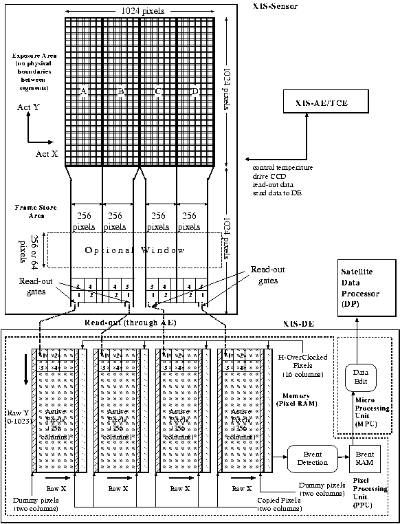
Figure 1 ( gif or postscript ) describes a schematic view of a single XIS CCD chip and its data transfer mechanism. X-rays focused by XRT are accumulated at the Exposure Area for a certain exposure period, and the data are transfered to the Frame Store Area after each exposure. Data stored at the Frame Store Area are read out sequentially and put into the on-board memory named Pixel RAM.
A single XIS CCD chip consists of four Segments (marked A, B, C and D in figure 1) and correspondingly have four separate read-out gates. Pixel data on each Segment are read-out from the corresponding read-out gate and sent to the Pixel RAM. In the Pixel RAM, pixels are given X and Y coordinates for each Segment in the order of the read-out, such that X values are from 0 to 255 and Y values are from 0 to 1023. These coordinates are named RAW X and RAW Y coordinates.
In the same Segment, pixels closer to the read-out gate are read and stored in the Pixel RAM earlier. Hence, the order of the pixel read-out is the same for the Segment A and C, and for the Segment B and D, but different between these two Segment pairs, because of the locations of the read-out gates. In figure 1, numbers 1, 2, 3 and 4 marked on the four pixel regions on each Segment indicate the order of the pixel read out from the chip and storage to the Pixel RAM.
Event detection is performed on the RAW XY coordinates for all the pixels by comparing pulse heights from the 3 x 3 pixels centering at each pixel. If the pulse-height from the central pixel is the highest, the RAW XY coordinates of the central pixel are considered the location of the event and sent to the telemetry. In order to enable the event detection on the rim of each Segment, two columns of pixels are copied to each Segment from the adjacent Segment (marked ``copied pixels'' in figure 1). In addition, on both sides of the outer Segments, two columns of empty ``dummy pixels'' are attached. Coordinates of the copied pixels and dummy pixels do not appear in the telemetry.
Actual pixel locations on the chip are calculated from the RAW XY coordinates and the Segment ID. The coordinates to describe the actual pixel location on the chip are named ACT X and ACT Y coordinates. The pixel read-out order has to be taken into account to calculate ACT XY from RAW XY. In addition, RAW XY to ACT XY conversion depends on the on-board data processing modes.
On-board Data Processing
There are two different kinds of XIS on-board data processing modes. The Clock modes describe how the CCD clocks are driven and determine the exposure times and time resolutions. The Editing modes specify how detected events are edited and determine the formats of the XIS data telemetry.
Clock Modes
- Normal Mode:
If Window option (see below) is not specified,
exposure time is 8 seconds, and all the pixels on the
CCD are read out every 8 seconds.
- Parallel Sum Mode: Pixel data from plural rows are summed in the Y-direction, and the sum is put in the Pixel RAM as a single row. The number of rows to add is commandable. Parallel Sum mode can be used only with the Timing edit mode (see below), and the Y coordinate is used to determine the event arrival time. No spatial resolution in the Y-direction.
Window and Burst option
For the Normal clock mode, Window and Burst option can modify the effective area and exposure time, respectively. The two options are independent, and may be used simultaneously.- Burst Option:
All the pixels are read out every 8 seconds
(if Window option is not specified),
but exposure time can be chosen arbitrarily
(with 1/32 second step) below the read-out interval.
This mode may be used to avoid the event pile-up when
observing bright sources.
- Window option : The Window option allows shorter exposure times using only a part of CCD to expose. Only a part of the chip in the Y-direction specified by the commandable Window is used for exposure. The Window width in the Y-direction is either 256 or 64 pixels, and its position is arbitrary. When the Window width is 256 pixels, the exposure time becomes a quarter of that without the Window option, and the Pixel RAM is filled with the data from four successive exposures. When the Window width is 64 pixels, the exposure time becomes 1/16 of that without the Window option, and the Pixel RAM is filled with the data from 16 successive exposures.
The following table indicates how the effective area and exposure time are modified by the Burst and Window options.
| Normal Mode without options |
Burst Option |
Window Option |
Burst & Window Option |
|
| Effective Area |
Nominal (25x25 square mm) |
Nominal (25x25 square mm) |
Lower (1/4 or 1/16) |
Lower |
| Exposure Time |
8 sec |
Lower |
2 sec x 4 exposure or 0.5 sec x 16 exposures |
Lower |
Editing Modes
- 5x5 mode:
All the pulse heights of the 25 pixels centering at the
event center are sent to the telemetry.
- 3x3 mode:
Pulse heights of the 9 pixels centering
at the event center are sent to the telemetry.
In addition, a 16 bit pixel pattern is output which indicates
if pulse heights of the outer 16 pixels exceeded
the split thresholds or not.
Sum of the outer pixel pulse heights lower than
the split threshold is also output.
- 2x2 mode:
2x2 pixel heights including the event pixel (highest one),
as well as other surrounding pixel pattern information, are output.
- Timing mode: This is used only with the Parallel Sum clock mode. Pulse heights of the three pixels in the X-direction are summed if they are over the split threshold, and sent to the telemetry. In addition, Grades of the events are determined and output.
XIS Related Links:
- Suzaku XIS Page at MIT
- Suzaku XIS Page at Osaka University (in Japanese)
If you have any questions concerning Suzaku, visit the Feedback form.