

Effects of radiation damage
on SIS performance
T. Dotani and A. Yamashita (ISAS) and
A. Rasmussen (MIT)
and the SIS team
dotani@astro.isas.jaxa.jp
SIS performance is gradually degrading due to the accumulated radiation damage. The effects of radiation damage are extensive: changes of energy scale, energy resolution, and detection efficiency. Details of these effects are explained together with the related calibration issues.
1 Radiation damage
In the space environment, X-ray detectors are exposed to high energy particles. Particle flux is especially large in the South Atlantic Anomaly, and charged produce lattice defects in solid state detectors, such as the SIS onboard ASCA. The SIS utilizes X-ray CCDs, and lattice defects in CCDs mainly have two effects on performance: charge traps and dark current.
Lattice defects make an intermediate energy level in the forbidden band, and such an intermediate level can work as an electron trap. This means that if a charge packet encounters an empty trap during the transfer, an electron will be caught in the trap and is removed from the packet in the subsequent transfer unless it is released immediately. Thus traps lead to loss of electrons from the charge packet, and hence charge transfer efficiency (CTE) becomes lower than unity. In the case of the SIS, charge packets are typically transferred 10^3 times before read-out. Very small degradation of CTE (eg ~0.99999) will lead to significant loss of charge. Hereafter, we use charge transfer inefficiency (CTI [[equivalence]] 1-CTE) instead of CTE for convenience.
Lattice defects can also increase dark current. Even without X-ray (or optical light) irradiation some thermally excited electrons are accumulated in the pixel. This charge is called dark current. In the case of the SIS, dark current was negligibly small before launch compared to the typical size of charge packet produced by X-rays. However, dark current has been gradually increasing after launch due to accumulated radiation damage. The immediate effect of the dark current may be excess noise due to the statistical fluctuation of the dark current and hence degradation of the energy resolution. Note that dark current itself will not introduce an offset of energy scale in principle. The zero point of the energy scale is estimated onboard, but as seen later this onboard estimate is systematically low. A positive pulse-height offset is thereby introduced in the energy-pulse-height relation that turns out to be mode dependent.
Radiation damage brings a lot of changes in SIS performance, such as change of energy scale, energy resolution and detection efficiency through these two effects. These changes are described in detail in the following sections.
2 CTI measurements with Cas A
Because CTI causes systematic reduction of X-ray photon energy, we can use the reduction to measure the CTI. If we put an X-ray source having prominent and stable emission lines on several different positions on a CCD chip, the line center energies are expected to show small but systematic shifts depending on the source positions. We can estimate CTI from these systematic shifts. We selected the supernova remnant Cas A as a target for CTI calibration; it is bright and relatively compact, and has strong emission lines.
When we measure CTI, we should be careful about the relation between clock
speed and CTI. As explained in Section 1, CTI results from the charge traps.
Even if an electron is caught in a trap, it will not produce CTI if the
electron is released while the charge packet stays on the pixel. Therefore,
traps which easily release an electron will not contribute to CTI. At the other
extreme, if the trap is very slow in releasing an electron, it is effectively
kept filled and again contributes little to CTI. Thus, only the traps whose
time scale of releasing electron is comparable to the clock time scale is
expected to contribute significantly to CTI. In other words, we need to measure
CTI for each clock of CCD.
Figure 1
The SIS uses 3 kinds of clock: ST clock, parallel clock and serial clock. The function of each clock is explained in Figure 1. These three clocks have different periods (the time between "ticks"). The ST clock and the pixel clock are fast, but the parallel clock is slow. The periods of each clock are listed in Table 1.
| Clock | Period |
|---|---|
| ST clock | 37 usec |
| Parallel clock | 8.7 usec |
| Serial clock | 18.5 usec |
Observations of Cas A were carried out in August 1993 and July 1994. The SIS was set in 1-CCD faint mode in both sets of observations. In the 1994 observations, there were three pointings for each chip, but the data were taken only with the standard chips in 1993. Two out of three pointings are arranged to differ only in h/v-address. Thus we can measure the shift of line center energy due to parallel/serial CTI separately. The CTIs determined from the line center shifts are listed in Table 2. Although it was not obvious how CTI depends on the X-ray photon energy, we found that the data are consistent with constant CTI. In other words, charge lost by CTI is proportional to the original size of the charge packet. Parallel and serial CTIs were determined from the data in 1994, but ST CTI cannot be determined from 1994 data only because the number of transfers by the ST clock is the same for all the pixels. We determined degradation of the ST CTI by comparing 1993 and 1994 data, and converted the degradation to an absolute value assuming that the CTI was zero at launch and increased linearly with time. This assumption turned out to be good because serial/parallel CTIs determined from 1993 and 1994 observations are consistent with no CTI at launch.
| Sensor | Parallel CTI | Serial CTI | ST CTI* |
|---|---|---|---|
| Chip | (x10^[-5] tr^[-1]) | (x10^[-5] tr^[-1] | (x10^[-5] tr^[-1]) |
| s0c0 | 2.85+/-0.38 | 3.07+/-0.50 | - |
| s0c1 | 2.31+/-0.18 | 3.09+/-0.22 | 1.37+/-0.39 |
| s0c2 | 3.19+/-0.28 | 2.57+/-0.39 | - |
| s0c3 | 2.39+/-0.38 | 6.47+/-0.51 | - |
| s1c0 | 3.42+/-0.31 | 6.20+/-0.51 | - |
| s1c1 | 2.14+/-0.30 | 2.83+/-0.40 | - |
| s1c2 | 2.13+/-0.35 | 5.22+/-0.49 | - |
| s1c3 | 2.38+/-0.20 | -0.23+/-0.25 | 2.53+/-0.51 |
*Estimated value assuming that ST CTI increases proportionally to time after the launch.
The above determination of CTI assumes that CTIs are uniform over the chip. However, we suspect that there may be significant variations of CTI over the chip. Negative values of serial CTI in S1C3 may be due to this non-uniformity.
3 Relative gain
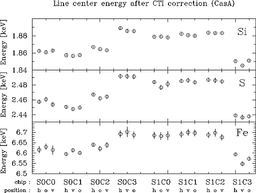
In the previous section, we used only the difference of line center energies to determine the CTIs. It is a different problem whether or not line center energies become consistent between chips after CTI correction. Figure 2 shows the line center energies of Si K[[alpha]], S K[[alpha]] and Fe K[[alpha]] of Cas A obtained with 1994 data after CTI correction.
Figure 2 Line center energies of Cas A after CTI correction. CTI values used were determined from the same observations (1994 data). Three data points in a chip correspond to three different pointings, denoted as h, v, and o. Line center energies in a chip are almost same, which means consistency between CTI determination and correction.
It is clear from the figure that the line center energies are different from chip to chip by at most 2%. However, we adjusted the relative gain of chips to better than 0.5% using W49B data in 1993. So, some systematic errors which we were not aware of should have been present in the gain calibration with W49B (this systematic error is explained in the next section). This motivated us to monitor the long-term history of the gain.
4 Gain history
Ni fluorescence lines in the SIS background are effectively the only structure in the energy spectrum available to monitor long-term history of the gain. Because 1-CCD mode data were taken only with standard chips, we accumulated the Ni line data only for the standard chips. Ni line data were accumulated from all the available data until November 1994 except for those close to the bright Earth or including bright target in the FOV.
There is one thing we need to keep in mind when we analyze Ni line data. The Ni line is believed to originate from the kovar which covers the frame store region of the chips (see figure 2 on page 6 in ASCANews no.2). However, some part of the Ni line was suspected to originate in the exposure region. The ratio of the Ni line flux between the exposure region and the frame store region can be determined in principle by comparing the Ni line fluxes of 1-CCD and 4-CCD modes. When we compare the fluxes, we need to correct the decrease of the detection effeciency due to RDD (see Section 7). We found that the flux ratio is F^(FS)_Ni ): F^(IM)_Ni) ~ 3 : 1, where F_Ni is defined as a flux in unit area (not pixel).
We cannot directly correct CTI for Ni line events because the number of transfers is not known for events produced in the frame store region. However, we can estimate the average shift of Ni line energy ([[Delta]] ENi) due to CTI using the flux ratio (F(^FS)_Ni : F^(IM_Ni) ) estimated above. In what follows, CTI correction for Ni line is done by simply adding [[Delta]] ENi to the apparent center energy of the Ni line.
Figure 3 Long-term history of Ni line energy for standard chips in 1-CCD mode (Figure 3a) and in 4-CCD mode (Figure 3b). Broken lines are apparent Ni line center energy and solid lines are that corrected for CTI and systematic energy shift in frame store region due to different pixel size. The dotted line is the expected K[[alpha]] line energy from neutral Ni (7.4723 keV).
The long-term history of the Ni line energy is shown in Figure 3. The Ni line energy in 1-CCD mode is almost constant after CTI correction, although there is a slight indication of annual variations. Systematic difference from the expected Ni K[[alpha]] line energy may be a calibration error. The difference of the gain between s0c1 (sensor 0, chip 1) and s1c3 (sensor 1, chip 3) is about 0.5% and is consistent with the Cas A results. On the other hand, 4-CCD mode data show clear contrast. The apparent line energy is almost constant, which means it increases after CTI correction. The difference of Ni line energies between 1 and 4-CCD modes is as large as 100 eV by the end of 1994. These results agree surprisingly well with the expected systematics stemming from zero-level errors outlined in the following section, specifically the upper panel of Figure 6. Thus, the constancy of the apparent Ni line energy (in 4-CCD mode) is very likely to be due to competing effects of CTI and the RDD. However, it is desirable to have independent measurements of CTI in 4-CCD mode (and also in 2-CCD mode), which is planned in August 1995.
The discrepancy between Ni line energies for 1- and 4-CCD mode may explain the calibrated gain error between chips (Figure 3): The W49B data used to calibrate gains were gathered from the various clocking modes. However, the subtle, mode- dependent systematics were not corrected for in the analysis, so it is certain that the unremoved systematics translated into small gain calibration errors.
5 Residual dark distribution
SIS Image data usually contain a small number of X-ray and charged particle events and most of the pixels are blank. The zero level of the energy scale, or dark level, is calculated onboard as an average pulse height of blank pixels. Only the blank pixels whose pulse height falls between -40 ADU and 40 ADU are used for this calculation. Dark level is calculated for a region of 16x16 pixels to accommodate the global variation of dark level over a chip. Onboard calculation of the dark level sometimes can not follow up the rapid change of the dark level due to the optical light leak, and this produces so-called dark frame error (DFE). DFE can be in principle corrected in the course of ground data analysis for faint mode data. The dark level of individual pixels has a statistical fluctuation around the global mean. In the ideal case, this fluctuation has a gaussian distribution and the width of the distribution corresponds to the read-out noise of the CCD.
Radiation damage increases the dark current. This means that blank pixels tend to have higher pulse height. However, a global increase of the pulse height of the blank pixels does not affect the energy scale, because the zero level of the energy scale is determined as an average of the blank pixels. The problem is the increased scatter of dark levels among pixels. We found that the dark level distribution became wider and asymmetric with increasing radiation damage. We refer to this distribution which remains after DFE correction as residual dark distribution (RDD).
Figure 4 Examples of the residual dark distribution (RDD) in 1-CCD and 4-CCD modes at two different epochs. Normalization of the plot reflects exposure time and source flux, and should be regarded as arbitrary. The solid line is the best-fit model function (eq. 1).
Examples of the RDD are shown in Figure 4. These are corner pixel distributions of grade 0, 2, 3, 4 events in faint mode data after DFE correction. The corner pixels of these grades are considered to be almost free from charges produced by X-rays or charged particles. Therefore, the pulse height distribution of corner pixels is a good approximation of the RDD. RDD is wider and more asymmetric in 4-CCD mode than in 1-CCD mode. This is natural because longer exposure (16 sec for 4-CCD mode and 4 sec for 1-CCD mode) means larger dark current. Similarly, recent data show larger asymmetry than the older data. It may be worth mentioning that RDD is closely connected to flickering pixels. The high energy tail of the RDD extends beyond the event threshold (=100 ADU). This means that some pixels have large dark current which can mimic an X-ray event. Thus the flickering pixels are in fact just the high energy tail of the RDD. In this sense, pixels with large dark current are sometimes referred to as micro-flickering pixels.
We found that RDD can be approximated by the following model function.
 (1)
(1)
This model function is a convolution of a d-function plus an exponential hard tail with a gaussian of width [[sigma]]. Fraction (f) represents the ratio of micro-flickering pixels, centroid (q0) is the true zero of the energy scale, and the exponential scale (Q) is a measure of the accumulated charge with RDD.
RDD has various effects on SIS performance. We explain systematics brought by the RDD in detail in the following sections.
6 Energy scale shift
RDD brings two kinds of effect on the energy scale. One is a zero level offset and the other is a systematic shift of line energy through the distortion of the line profile.
It is easily understood that onboard calculation of the dark level suffers from systematic offset due to the asymmetry of the RDD because the onboard calculation is just a truncated mean of the pulse height of blank pixels. This offset is further modified by data reduction at ground through DFE correction. DFE correction software cross-correlates the corner pixel distribution of the data being processed and a template distribution. The template is in fact a corner pixel distribution of 1-CCD data in early 1993 and hence its distribution is almost symmetric and peaked close to zero. Thus the current DFE correction effectively aligns the distribution peak close to zero, which is always less than the truncated mean: the effective DFE "correction" correspondingly introduces a positive pulse height offset equal to this difference. Thus, while the on-board dark level underestimates the "best" zero level, the current DFE correction underestimates it by a larger measure: the offset in the gain solution is inflated as a side-effect of using FAINTDFE. Incidentally, this is no accident. The original need for FAINTDFE was to align data for which the dark level calculation was out of equilibrium. In order to align faint mode data, for example, with bright mode, with a significant equilibrium DFE, appropriate models for the cross-correllation template must be used.1 These templates are currently under development and testing for use with FAINTDFE.
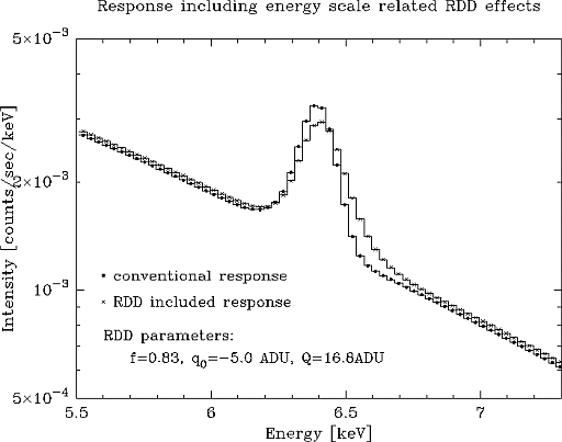
Figure 5 Line profile change due to RDD for grade 0 events. Simulated energy spectrum of SIS is shown for a model of a power law (photon index 1.7) plus a narrow line. Note that only the RDD effect related to the energy resolution is demonstrated here; degradation of the detection efficiency is not simulated.
The RDD also changes the line profile. The usual line profiles were originally determined by considering effects of charge generation, drift and collection, readout noise and details of the ASCA SIS event selection and pulse height recipes. Because an incident X-ray strikes a CCD pixel and thereby samples the RDD at random, the line profiles may still be predicted, provided that the readout noise distributions are replaced by the RDD everywhere. A line profile should still exhibit a low pulse height shoulder located within about a split threshold (~ 140 eV) of the peak, but as the RDD becomes broader and less symmetric, the profile grows a tail on the high pulse height side. Thus the line profile may become approximately symmetricby coincidence. We show a simulated spectrum of SIS in Figure 5 to demonstrate the RDD effect on the line profile. Note the high energy tail of the line profile and the shift of the line center. The decrease of the detection efficiency due to RDD (see Section 7) is not included in this demonstration.
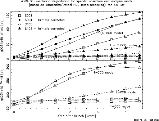
Figure 6
The current versions of SIS response matrices do not include the RDD effects. Thus, if we fit an energy spectrum affected by RDD with a model function, the line center energy suffers from a systematic shift. As mentioned above, the RDD effectively underestimates the "best" zero, and the first moment of the response undergoes a systematic shift in the positive pulse height direction. Figure 6 (upper panel) shows the expected systematic offset of the line center energy due to the RDD for a narrow line at 6.6 keV in various clocking modes. The amount of the shift is not very sensitive to the line energy. As seen from the figure, DFE correction increases systematic offset of the line center energy.
Figure 6 also shows the degradation of the energy resolution due to the RDD at 6.6 keV. RDD is much broader than the distribution of the read-out noise at launch and hence degrades the energy resolution. Although FWHMs for DFE-corrected data are not shown here, we expect moderately worse resolving power for this grade combination: For a given grade, the DFE correction introduces only a shift in pulse height, so the resolution should not be affected. In the standard grade combination g0234 however, we combine single-pixel pulse height calculations with two-pixel calculations, so the pulse height shift carries along with it an additional broadening. This broadening is certainly energy dependent, because the grade branching ratios vary with energy.
7 Detection efficiency
RDD not only changes the energy scale/resolution of SIS, but also changes the detection efficiency. An X-ray photon produces a charge cloud which extends at most a few pixels. The onboard processor looks for a pixel which exceeds the event threshold (=100ADU ~ 0.35 keV) and, if found, examines neighboring 8 pixels. If the pixel is a local maximum among 3x3 pixels, it is regarded as an event. Further processing may be done by the onboard processor (bright mode) or on the ground (faint mode). The surrounding 8 pixels are compared with the split threshold (=40 ADU), and the events are classified into grades according to the number and pattern of pixels which exceed the split threshold. If no pixel exceed the split threshold, the event is classified as grade 0, and higher grade is assigned to event which have larger number of pixels exceeding the split threshold. Because X-ray events usually do not extend more than 4 pixels, high grade events are regarded as non X-ray events. In the case of the SIS, grades 1, 5, 6, and 7 are regarded as non X-ray events.
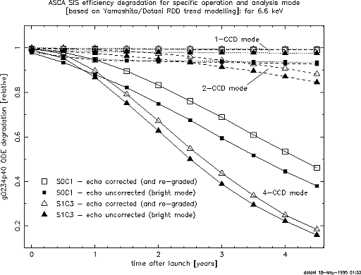
Figure 7
The RDD effect increases the probability of a pixel exceeding the split threshold. Lower grades of events, which are mostly X-ray events, may become higher grade of events if some of the 8 surrounding pixels exceed the split threshold. If X-ray events are changed to grades 1, 5, 6, 7, they are regarded as non X-ray events and hence removed from later processing. Thus the RDD effect alters the grade branching ratio and hence detection efficiency of the X-ray events. Figure 7 shows the long-term variations of the detection efficiency due to RDD at 6.6 keV. Reduction of the detection efficiency is most prominent in 4-CCD mode data without echo correction. In the case of 1-CCD mode data, only the reduction of detection efficiency due to the echo is seen. Increase of the echo ratio was saturated by about a year after launch.
To illustrate the overall effect of the RDD on the SIS broadband response, we show in Figure 8 several semi Monte Carlo spectra of 3c273 in various clocking modes. Because 1-CCD mode data are little affected by the RDD, we can get a rough idea how RDD modifies the apparent energy spectrum by comparing 1-CCD and 4-CCD results. Detection efficiency is reduced in overall energy range and the instrumental sharp structures in the spectrum (oxygen K, silicon K, and gold M edges) are smoothed out due to the degraded energy resolution. In addition, the low-energy efficiency suffers substantially as a significant fraction of the response profile falls below detection threshold. This is a direct result of the asymmetric RDD: down-shifted pulse height medians close to pulse height thresholds are stochastically rejected, which effectively smears out and inflates these thresholds. Noninflated thresholds currently stand at 120 and 160 ADU in 4-CCD mode, corresponding to 440 and 580 eV for single pixel and two-pixel events, respectively.
8 Calibration database and analysis software
To cope with the degradation of SIS performance due to radiation damage, updates of calibration database and analysis software are now in progress.
Gain
Because the relative gain between chips was calibrated using all 1/2/4-CCD mode data of W49B, which are now known to have different CTI/RDD effects, it includes relatively large systematic error. As explained so far, we have calibrated the gain with Ni line in the background and Cas A observations. The new gain will be released after consistency check with the previous calibration.
Figure 8 Simulated spectra of 3c273 (in December 1993) in various clocking modes at two different epochs. Left panel shows the spectra expected at 2 years after the launch, and right panel those of 4 years after the launch. These histograms are of actual flight faint mode (3 x 3) data. Expected RDD effects were introduced by Monte Carlo corruption of all pixels, such that the corner pixel distributions are consistent with current, best projections (by Yamashita and Dotani) of the RDD evolution. Naturally, this includes the RDD-driven, self-consistent onboard zero level error. Onboard processing of this data was also simulated to produce these histograms.
DFE correction
The current program of DFE correction introduces a systematic offset in the energy scale when applied to the data with RDD. We need to use an appropriate template depending on the clocking modes and time after the launch. Because the template is in fact RDD itself, we can use the model function in equation 1. We have found analytic formulae which can describe the long-term variations of the parameters in equation 1 for 1/2/4-CCD modes. The new DFE correction program will use the model function, which is determined by the clocking mode and observation time, as a template.
CTI
CTI in 1-CCD mode was measured with Cas A data. But, as explained in Section 4, CTI may depend on the clocking mode of CCD. Because we do not have appropriate data to determine the CTI in 2/4-CCD modes, we are planning to observe Cas A once again in August in 1995. CTI in 2/4-CCD modes will be determined with these new data.
Response matrices
Because RDD effects are not easy to correct at ground data processing, the effects should be included in the response matrices. This means that SIS matrices would become clocking mode and time dependent. The effort of upgrading the response builder is continuing.
Conclusion
We have made substantial progress in understanding the effects of radiation damage on SIS performance. As has been shown in sections 6 and 7, the RDD has degraded 4-CCD mode data so as to make this mode unusable; 2-CCD mode may also become unusable in the foreseeable future. Unfortunately, this severely limits the scope for future observations of extended sources with the SIS. However, 1-CCD mode continues to function well and, therefore, point source observations are affected little. We will be issuing updated calibration software and data, notably a new response builder that generates time and mode dependent matrices, to enable more accurate analyses of the existing SIS data.
[1]See ftp://benz.mit.edu/asuka/sis/rdd/RDD_memo_6_16_94.ps for details regarding these models and a thorough analytical formulation of the RDD.
 Proceed to the next article
 Return to the previous article
 Select another article
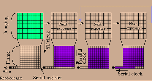